50 Mbps UART in an FPGA: my intro into FPGA
I was wanting to learn a little about FPGA and was wondering how fast I could make a UART (universal asynchronous receiver transmitter) go with an FPGA (field programmable gate array). It seemed like a good learning project. Having a quick look I saw that the XR17V352 chip can do 31.25 Mbps so I ideally wanted it to go faster than that.
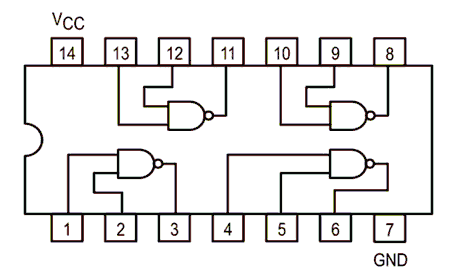
I have never worked with FPGAs before so it is been a large learning curve. FPGAs contain lots of little configurable logic elements that can be joined together and configured to do what the user wants. FPGAs mean you can create custom digital hardware. Apart from FPGA the alternative methods to create custom digital hardware is to either buy chips and connect them together with physical wires or get a chip designed and manufactured for you (the latter is called ASIC ). FPGA allows you to relatively easily reconfigure hardware compared to these two other alternatives. You don’t have to purchase more chips or dig out the soldering iron to reconfigure the hardware. Cost wise it’s far cheaper than ASIC that apparently can cost millions of dollars 1. Also with the FPGA chips around today you can make some very complicated hardware as these chips can have hundreds of thousands of logic elements in them; compare this to something like a 74HC00 which has only four NAND gates in it.
 74HC00 Internal Diagram
Pretty much any digital circuit can be made out of NAND gates if you’ve got enough of them, inverters, or gates, and gates, flip flops, even a CPU. To do this of course you have to wire them up and this has traditionally been with physical pieces of wire sold on the legs of the chips. With FPGA in contrast you can wire these gates up together in the FPGA chip itself without having to touch a soldering iron.
So I bought a development an FPGA board containing an EP4CE10E22C8N chip. This FPGA chip is called a Cyclone IV chip by Altera but has now been bought out by Intel.
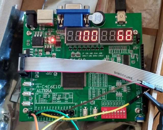 Altera/Intel Cyclone IV development board
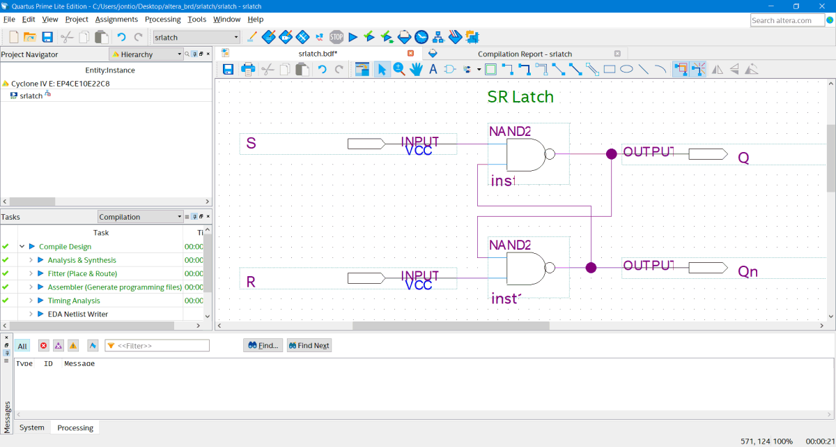
Initially before first using this board I thought it was rather archaic looking with LED segment displays and dip switches but it actually turned out to be an extremely useful board for learning on. The LCD segments and buttons are useful for getting started applications. One very useful thing I found was having the pin numbers written on the PCB silkscreen, this meant I didn’t have to look through the schematic when trying to figure out the name of a particular pin but could use the board itself when doing what is called the pin assignment. Anyway let’s try a simple hardware design using old school schematics of gates, how about an SR latch?
SR Latch
Let's put together an SR nand latch. It looks like the following...
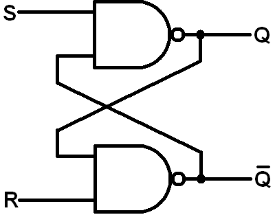 SR nand latch
These Altera/Intel FPGA seem to be designed and configured using a program called Quartus prime. So I downloaded and installed the lite version of that; version 20.1.0.
 Quartus prime light version 20.1
I don't like Windows 10!!! I find Windows 10 is buggy, bloated, controlling, manipulating, difficult for people with poor vision or mobility, and full of adware. I find Windows 10 and android rather similar these days and dislike them both. I later found out it ran fine on Linux so I’ll install it some other time on my Linux system. However, Windows is easier for me to do write ups and it’s the only operating system I can use Dragon NaturallySpeaking which I absolutely need for emails and writing. Anyway back to the point I put it on a Windows 10 install. Let’s create the project using the new project wizard, it just requires filling in a few things and pressing next a few times…
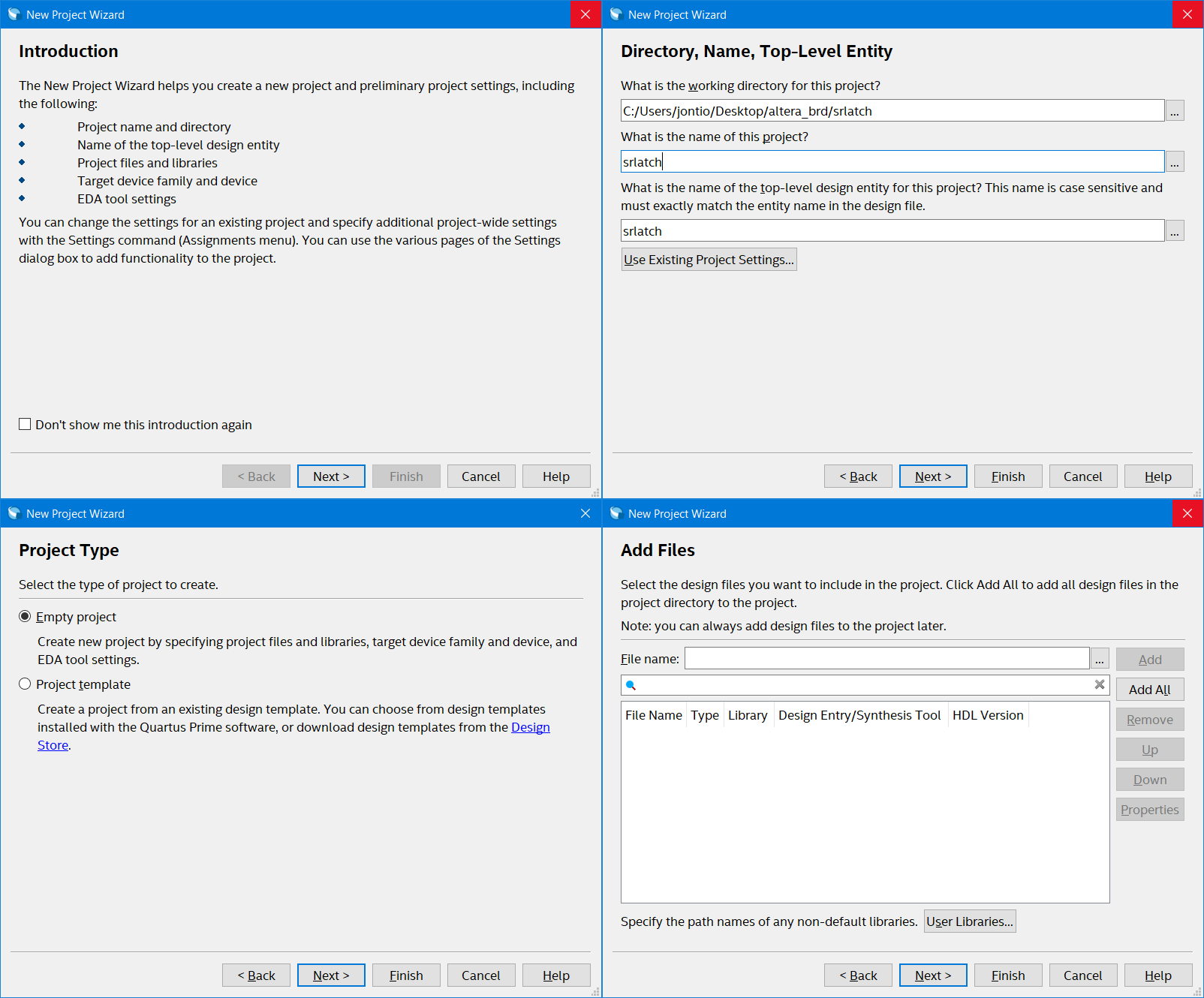 New project wizard part one: lots of nexts
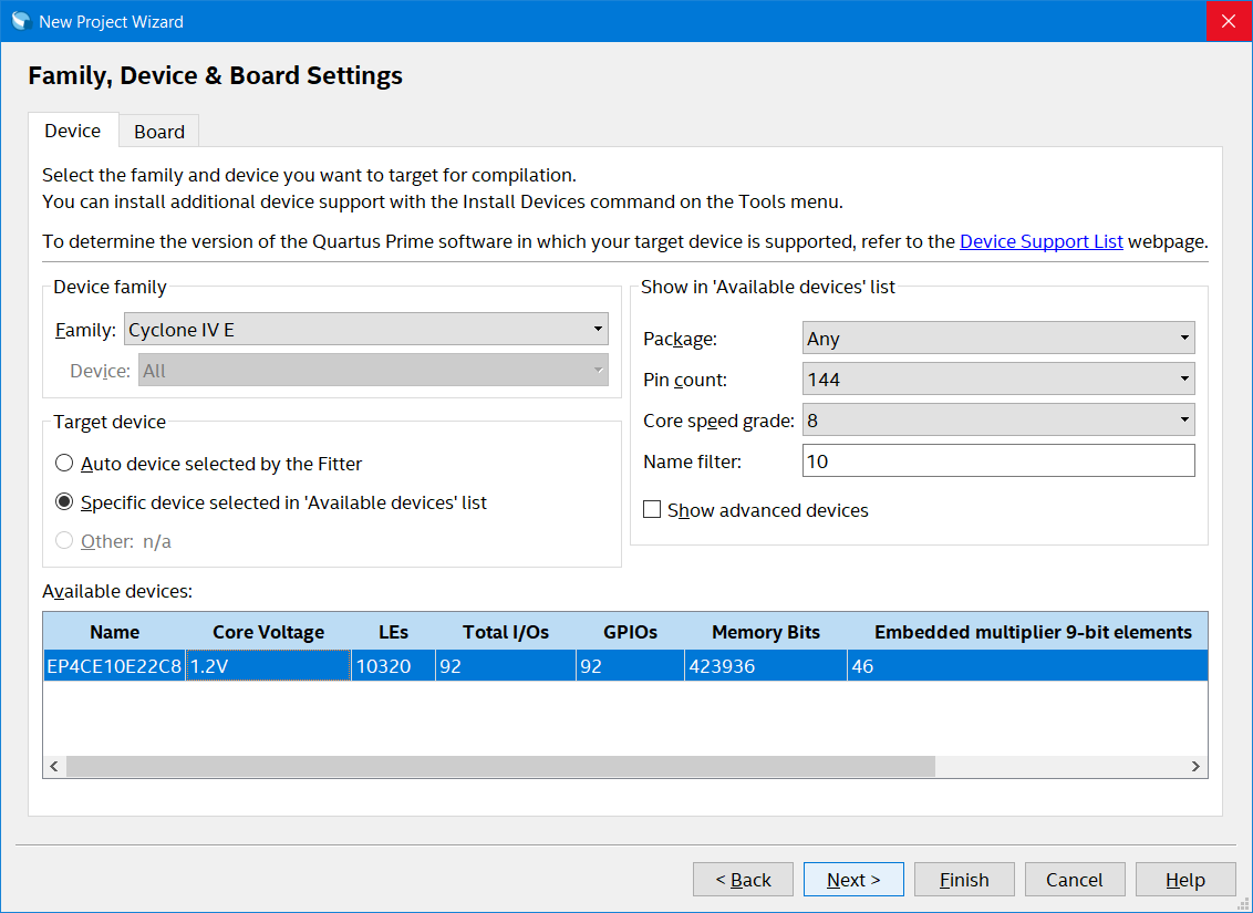 New project wizard part two: selecting the device
 New project wizard part three: more nexts
Then file → new → block diagram/schematic file
 Create a new schematic file
And now we can draw our schematic…
 Schematic drawing of the SR flip-flop
Then save it…
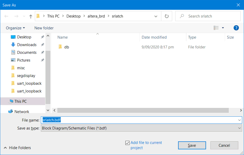 Save the schematic
Then processing → start compilation
It should complete with no errors.
Then assignment → pin planner
This is where the wires of the SR latch inside the FPGA are connected to the physical pins on the board. For the board I have P90 and P91 are pushbuttons while P72 and P73 are a couple of the LEDs on the board so these what I will use. I typed these numbers into the location boxes…
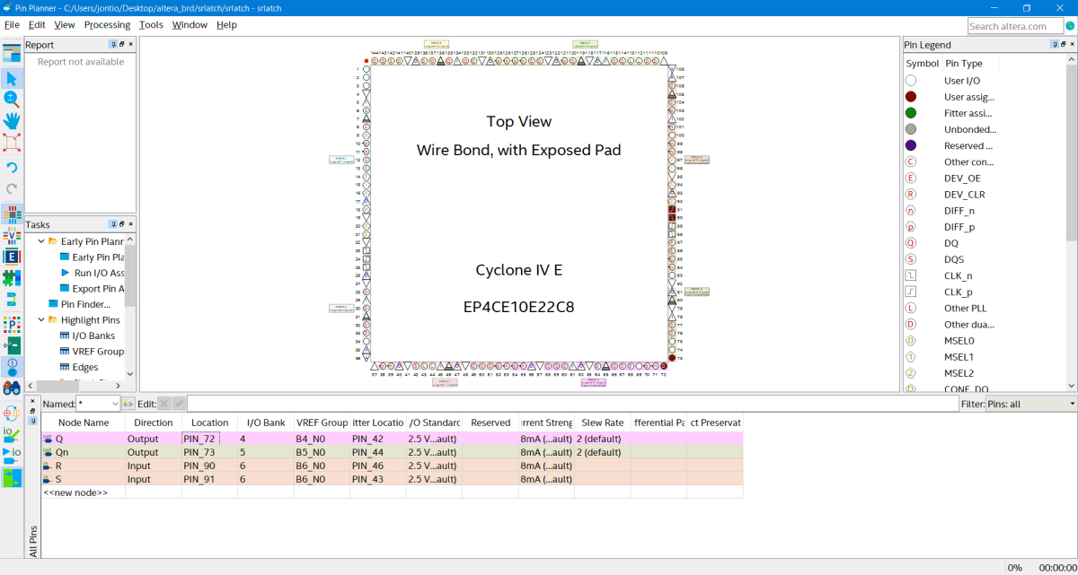 Pin planner: Assigning the SR latch to the outside world
Then close the pin planner (any changes will automatically be saved)
Then processing → start compilation again
Then tools → programmer
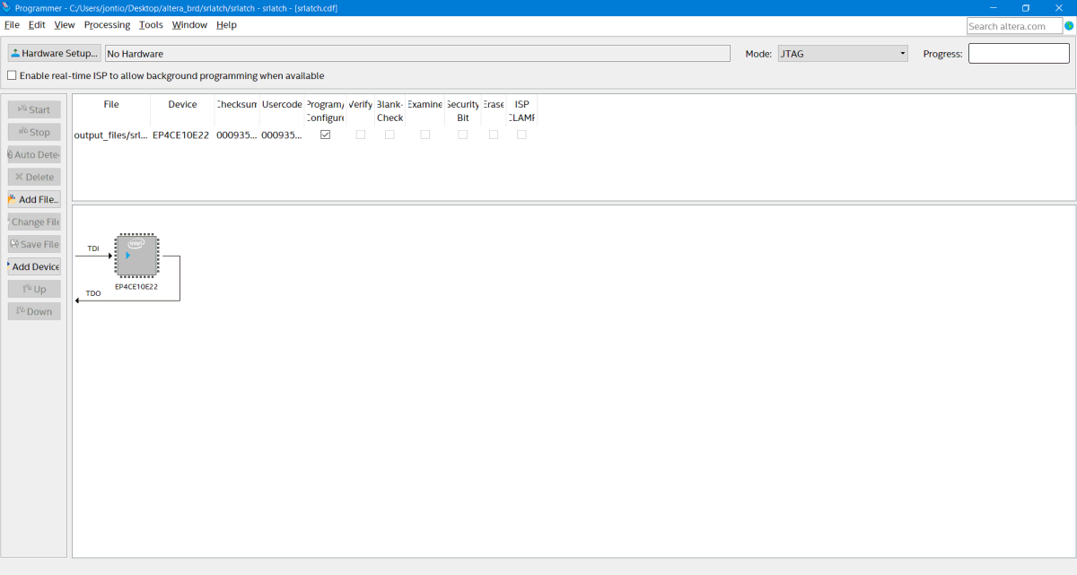 Programmer: Places the design in the FPGA
For some reason I get no hardware detected and have to remove the USB blaster then plug it in again then go to hardware set up before I can select my USB blaster…
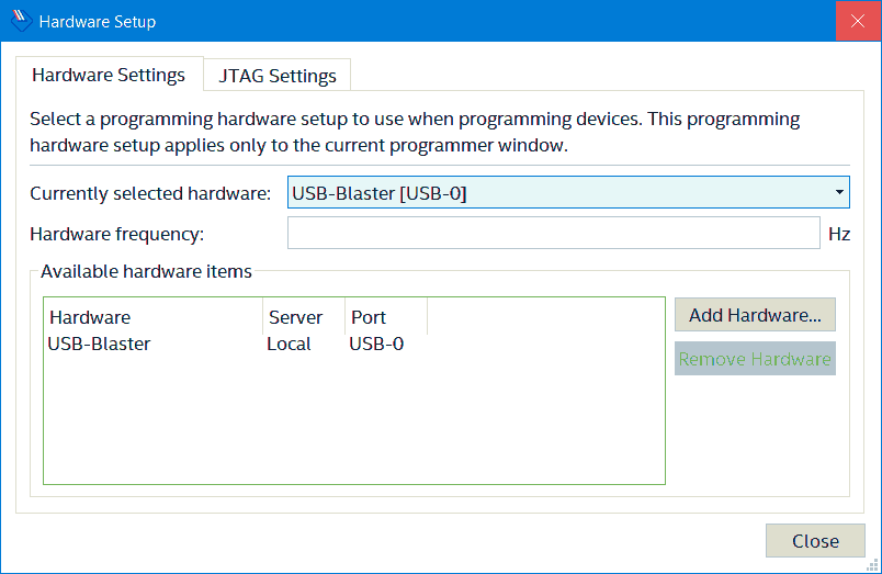 Selecting the Altera USB blaster
Now start is clickable and I click on it to write the design to the FPGA…
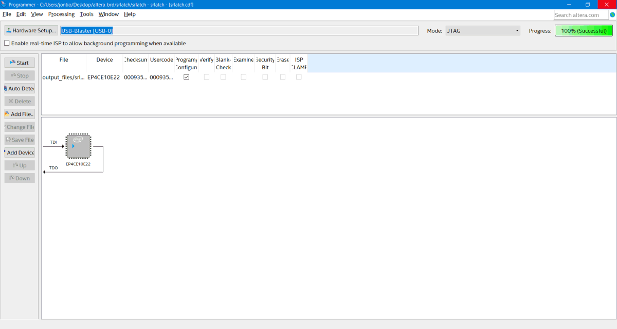 The design successfully written to the FPGA
So that then turns the FPGA into an SR latch where I can press one button and one of the LEDs lights and the other one goes out and when I press the other button the LEDs reverse.
Verilog
While you could write entire designs using schematics like this it would be difficult to write complicated hardware like this. This is where hardware description languages (HDL) come in. For me I chose to learn a little bit about an HDL called Verilog. Verilog is a subset of the language called SystemVerilog. There are various versions of Verilog, I assume I’m using the latest which I think is 2005? Verilog/SystemVerilog has things called modules that are effectively like little chips that do a particular task so if we wanted to make a SR latch in Verilog it could look something like this…
module srlatch(input S,R, output Q, Qn);
assign Q=~(S&Qn);
assign Qn=~(R&Q);
endmodule
To use this Verilog design you can go to the project navigator pain select files, right click the bdf file then select delete. Then file → new and select Verilog HDL file. Copy the code snippet from above into the text editor, then save the file as “srlatch.v”.
We can then compile it and then go to tools → netlist viewers → RTL viewer to see a schematic of what this Verilog looks like…
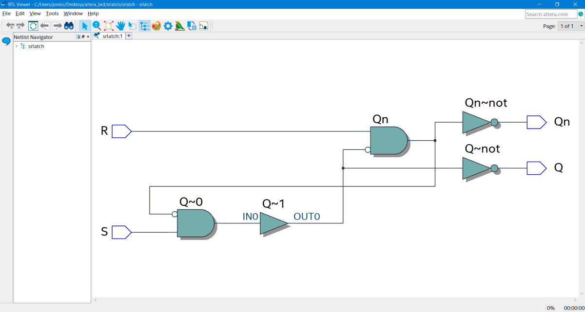 RTL view of the Verilog code snippet
It’s a bit strangely drawn but it’s the same thing.
RTL simulation
Simulation seems to be a large part of design validation. Without simulation it can be difficult to figure out what’s wrong with your design or if your design even works. Something called ModelSim comes with Quartus prime and seems to be a common simulator that people use; so I used it.
RTL (register transfer level) simulation seems to be the first thing to do and ignores real life timing delays caused by the gates. However, before doing RTL simulation with ModelSim you have to create a new project like we did with the project wizard before, create some sort of device, and then create something called a test bench.
So create a new project called “pll_and_flipflop” and add a Verilog file to it and save it as “pll_and_flipflop.v”. This time as well as simulating the design using a test bench I’d like to add a phase locked loop (PLL) to multiply the incoming clock frequency by five times then divide this by two times using a Flip-Flop. FPGAs as well as having gates on them usually have other bits and pieces such as RAM and PLLs. So far the only way I know how to use these kinds of things is by going to tools → IP catalog...
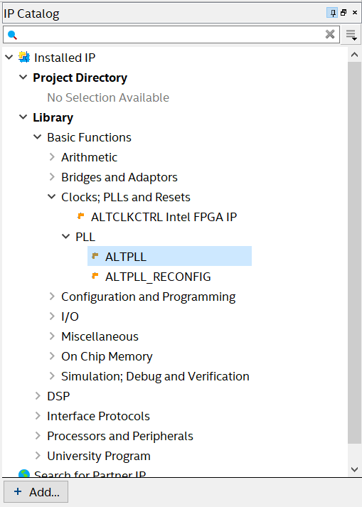 IP catalog in Quartus
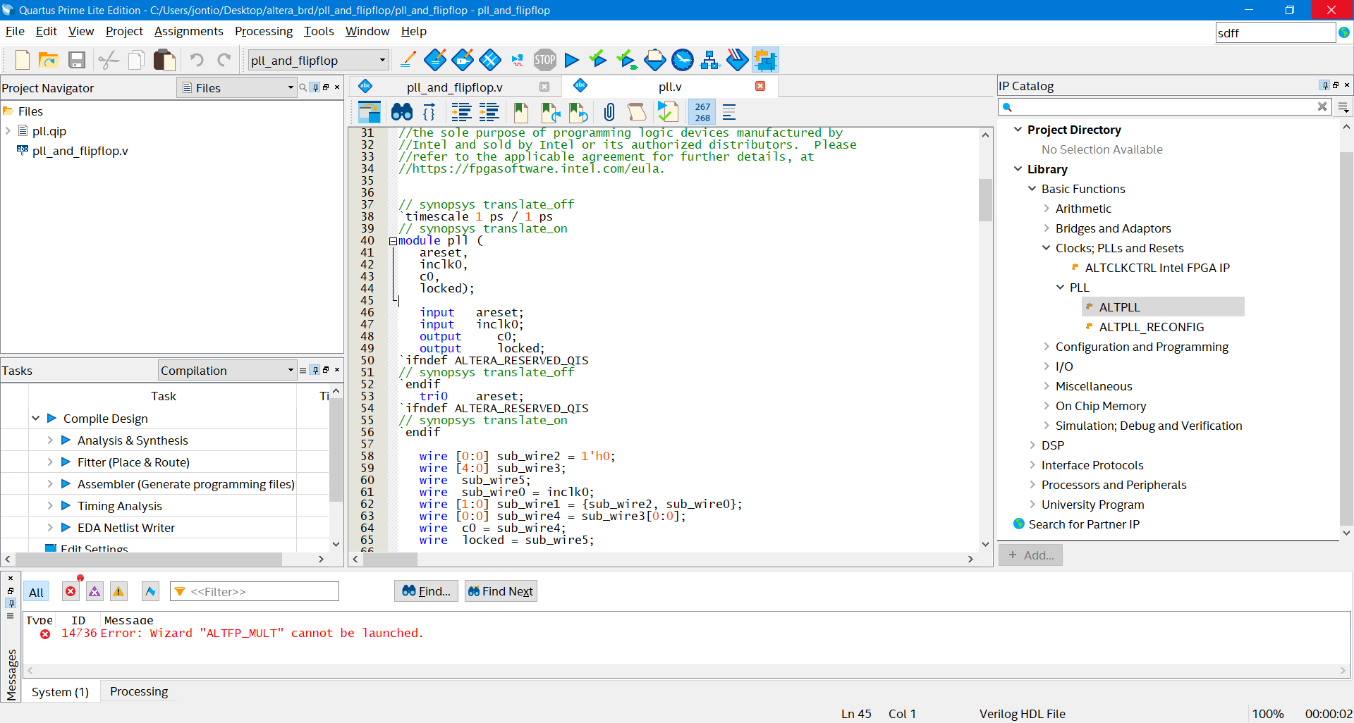
This brings up a bunch of things that can be added to your project. However, one of the first things I found out when trying to use these things was a lot of them just don’t work. For example under library → basic functions → arithmetic → altfp_mult I get the following unhelpful response…
Error (14736): Error: Wizard “ALTFP_MULT” cannot be launched.
The ALT that prefixes everything presumably means Altera. Some of these so-called mega wizards when you click on documentation take you to webpages that say file not found. I also didn’t find much community support for Quartus. To me it seems like Intel is neglecting the community scene. Xilinx on the other hand seemed to have a better community scene with people asking and answering questions. However, I have yet to use Xilinx so until I do I can’t say much about Xilinx. Anyway back to adding a PLL to our project. Double-click on ALTPLL and dialog box asking to save the IP variation as pops up. Save it as pll.v and of type verilog.
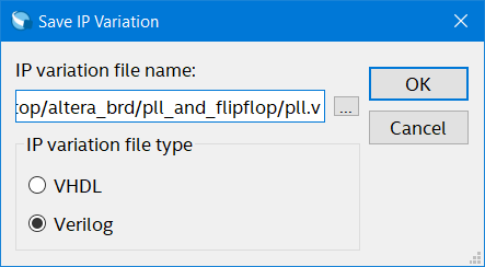 Save the IP variation
The ALTPLL mega wizard pops up…
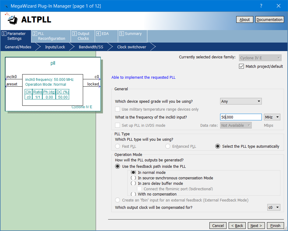 ALTPLL MegaWizard
I didn’t change much but I changed the input frequency to 50 MHz as that’s what the onboard oscillator is working at. I pressed next a few times ignoring what they were talking about…
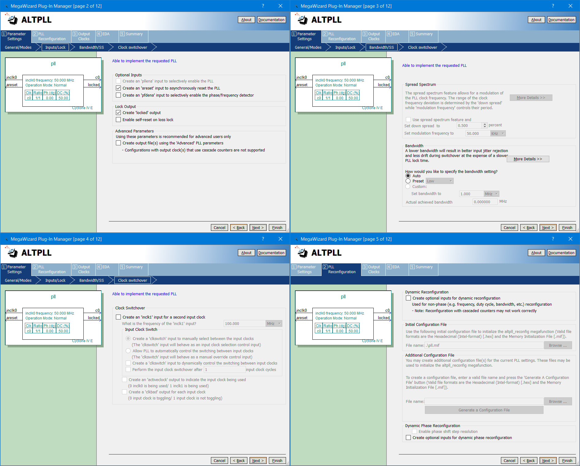 Ignoring this stuff
Until I got to the one where you could set the multiplication factor of the PLL, I sent this to five…
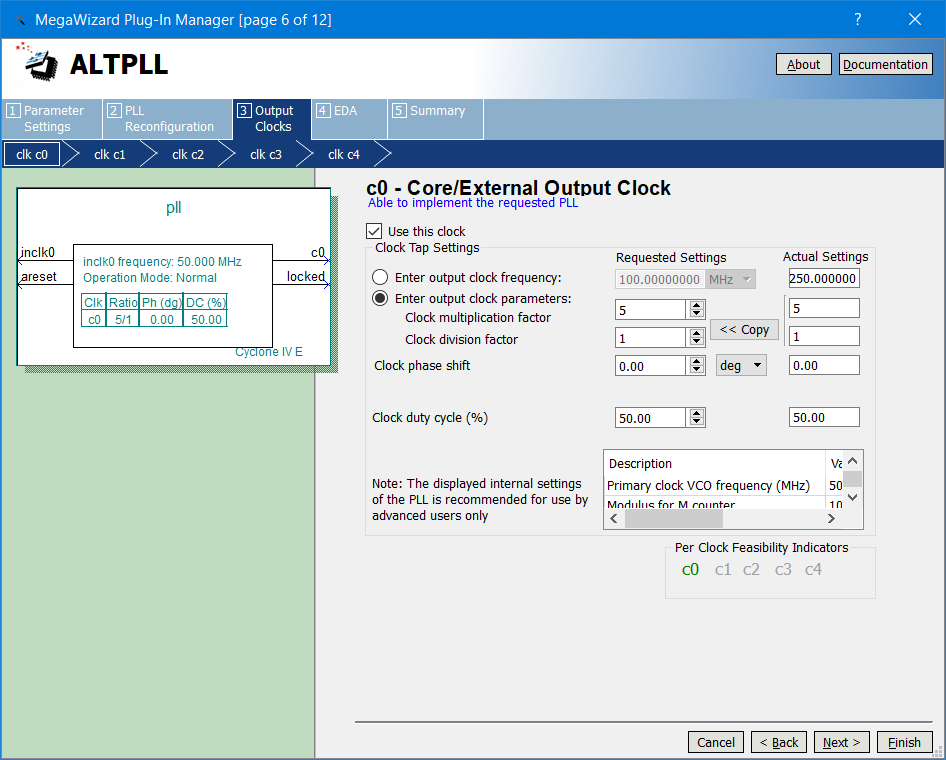 Set the PLL multiplication factor five
Then I just kept pressing next until I could go no further and then finally pressed finished. In the project navigator under files there’s something called pll.qip that can be expanded out and there you can see the file called pll.v…
 The file pll.v automatically created by the MegaWizard
The start of it around “module” is the useful bit for us as to how to use it…
pll (
areset,
inclk0,
c0,
locked);

	input	  areset;
	input	  inclk0;
	output	  c0;
	output	  locked;
It looks like an asynchronous reset, clock input, clock output and a wire to signify when the PLL is locked. So, back to our pll_and_flipflop.v file and design a flip-flop along with the magic pll module that has been designed for us. Copy the following into that file…
module pll_and_flipflop(
input clk_50, //50MHz input clock
output clk_250, //250MHz output from PLL
output reg clk_125, //output of flipflop driven by the PLL so that’s 125MHz
output locked //high when clk_125 and clk_250 are working correctly
);

pll pll0(
.areset(1’b0),
.inclk0(clk_50),
.c0(clk_250),
.locked(locked));

initial clk_125=0;//flipflop initially 0
always @(posedge clk_250)//on flipflop’s clk edge...
begin
	clk_125<=~clk_125;//...toggle it’s output
end
endmodule
Then create a test bench file called pll_and_flipflop_tb.v…
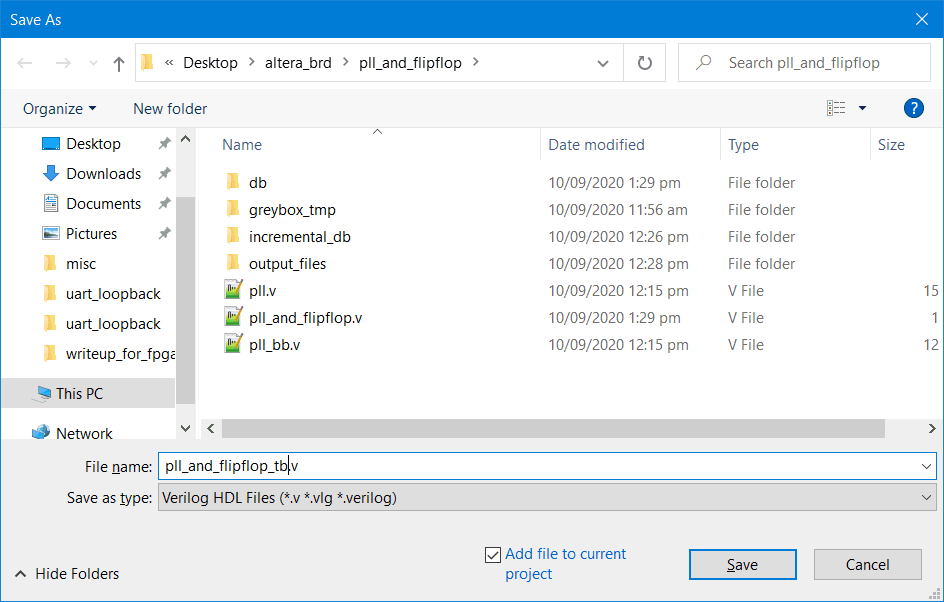 Create a new test bench file called pll_and_flipflop_tb.v
Instantiate the pll_and_flipflop device we just designed by putting the following into the test bench…
‘timescale 1 ps / 1 ps
module pll_and_flipflop_tb;
pll_and_flipflop
pll_and_flipflop0
(
.clk_50(clk_50), //50MHz input clock
.clk_250(clk_250), //250MHz output from PLL
.clk_125(clk_125), //output of flipflop driven by the PLL so that’s 125MHz
.locked(locked) //high when clk_125 and clk_250 are working correctly
);
Endmodule
Go to assignments → settings → EDA Tool settings. Then for simulation select "ModelSim-Altera"…
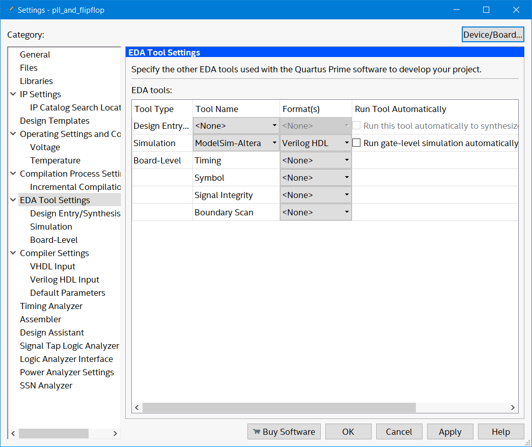 Select "ModelSim-Altera" for the simulation
Then simulation and click compile test bench…
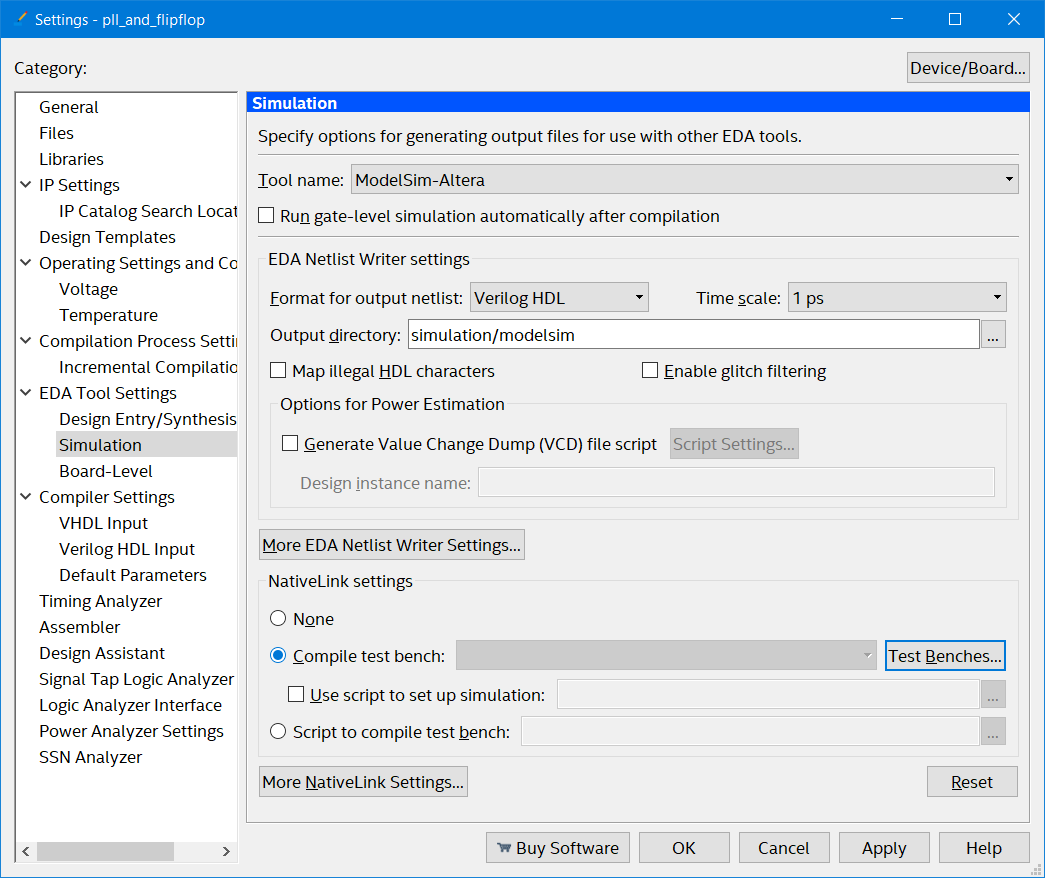 Select and click "Compile test bench"
Click test benches and add new…
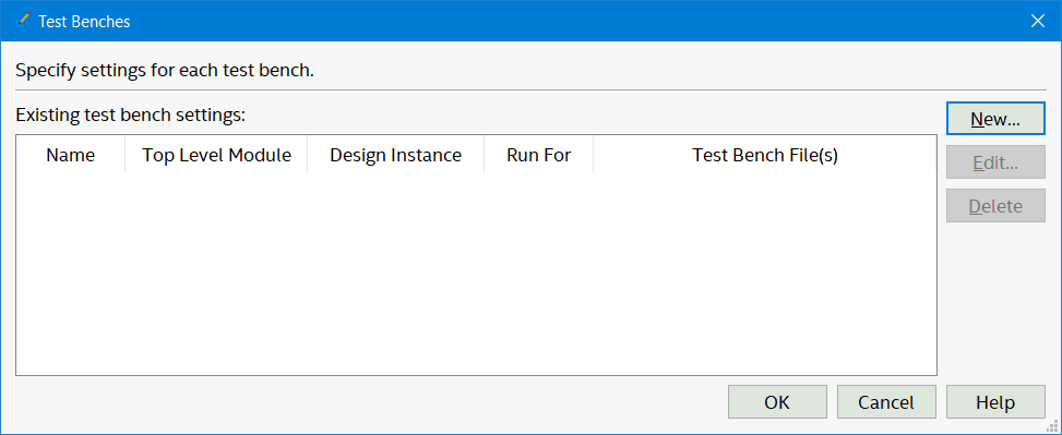 Add a "New" test bench
Add the test bench name and file…
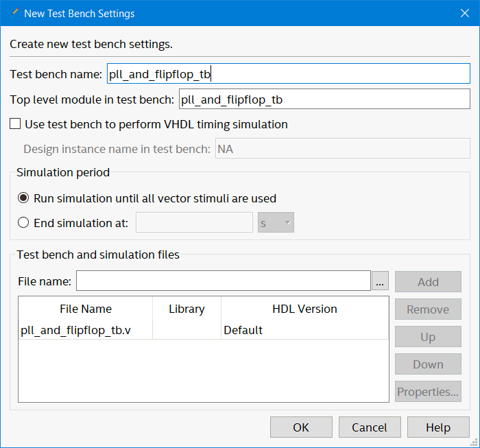 Add the test bench name and file
Then OK two times to get out of there.
At this point you could put the code you want the simulator to run into the pll_and_flipflop_tb.v file but so far most of the time I have found it more convenient to use a ModelSim script to take that role. So that’s what I’ll do here.
Next create a file called simdo.do (well whatever you want to call it but the extension should be .do). Then go back into assignments → settings → EDA Tool settings → settings and add the simdo.do file to it…
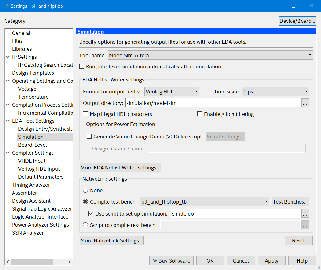 Add the simdo.do file to the simulation
Compile the project if you haven’t already done so and assuming it has compiled correctly go to Tools → run simulation tools → RTL simulation. That should start modelsim with the test bench…
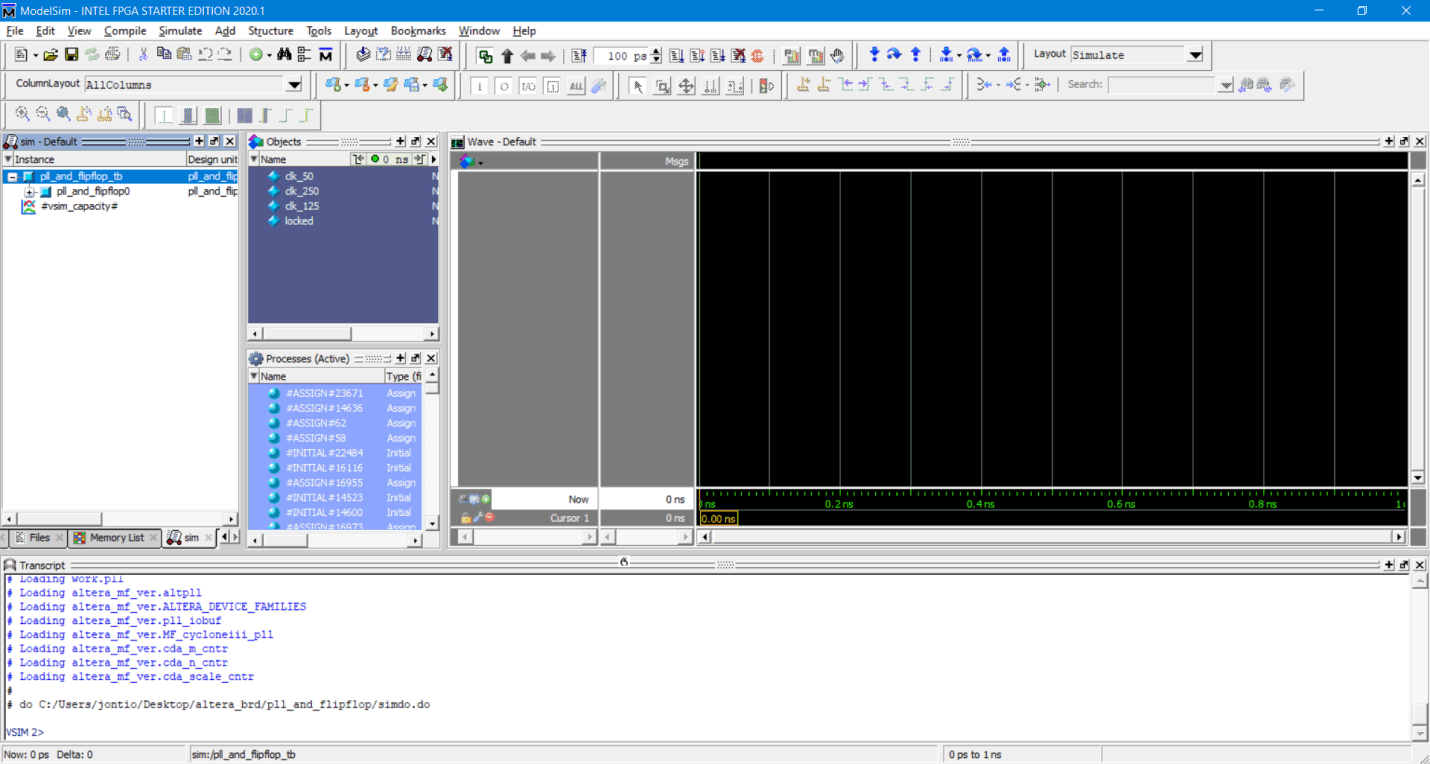 ModelSim starts
Right-click on the clk_50 signal in the objects window and add that signal to the wave window…
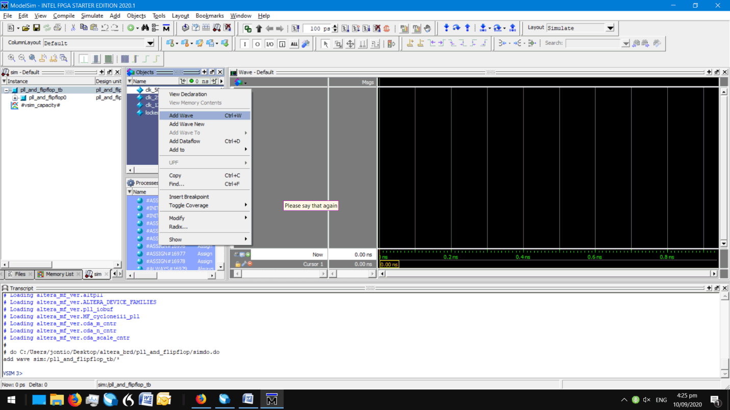 Add the clk_50 signal object to the wave window
Do that for the other three items in the objects window.
Most things you do and model some causes commands to happen that can be seen in the transcript window. The mouse clicks you just did actually just called the commands…
add wave -position end sim:/pll_and_flipflop_tb/clk_50
add wave -position end sim:/pll_and_flipflop_tb/clk_250
add wave -position end sim:/pll_and_flipflop_tb/clk_125
add wave -position end sim:/pll_and_flipflop_tb/locked
So we don’t have to go through this hassle of setting up ModelSim how we like it every time we run the test bench, instead we can copy these commands and put them in the simdo.do file so that they run when we start ModelSim next. If we look in the ModelSim manual we can read more about these commands and customize them. For example this add wave command has the following syntax…
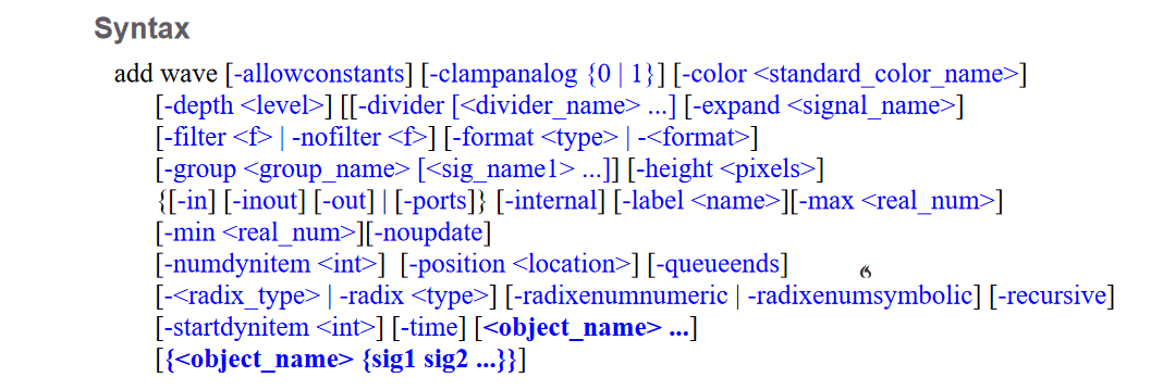 Add wave syntax for ModelSim
So let’s fancy up the display a bit. Copy the following commands to the simdo.do file…
add wave -divider “ Clock in “
add wave -position end -label “clk_50” -color “Magenta” 	sim:/pll_and_flipflop_tb/clk_50
add wave -divider “ PLL out “
add wave -position end -label “clk_250” sim:/pll_and_flipflop_tb/clk_250
add wave -position end -label “locked” sim:/pll_and_flipflop_tb/locked
add wave -divider “ FlipFlop out “
add wave -position end -label “clk_125” sim:/pll_and_flipflop_tb/clk_125
Save the file, close ModelSim, then start ModelSim again by going to Tools →run simulation tools → RTL simulation. This time there should be some things in the wave window.
Now we need the test bench to clock the input clock wire clk_50. To do that right click on clk_50 in the wave window then click on clock. Change the period to 20,000 which means 20,000 ps aka 50MHz (1/20000ps=50MHz) then click on OK.
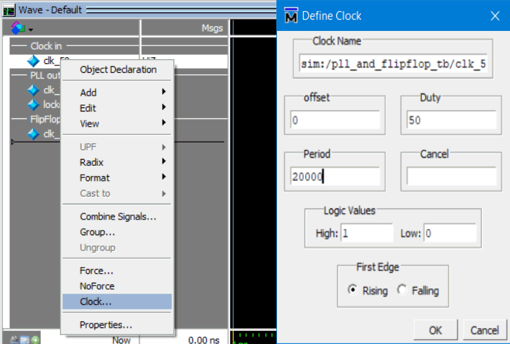 Add a clock stimulus to the simulation
If you click on simulate → run 100 the simulation will progress at 100 ps each time you press it. You can change the default run period time to say 100ns by entering it into the little box at the top of the window or going to simulate → runtime options and setting the default run period there.
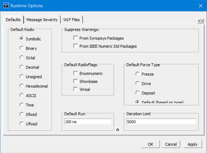 Set the run period to 100 ns
If you press run 100 enough you should see the lock signal become active and both the clk_125 and clk_250 signals will start to oscillate…
 Click "run 100" a few times
You can see the PLL is locked after 60 ns and the output of flip-flop is five cycles in a 40 ns period which equates to 5/40ns=125MHz as expected. We don’t have to do all this clicking and instead we can add this to our simdo.do file by adding the following to it…
force -freeze sim:/pll_and_flipflop_tb/clk_50 1 0, 0 {10000 ps} -r 20000
when -label “locked” {sim:/pll_and_flipflop_tb/locked==1} {echo {Break on locked} ; stop}
run -all
run 100000
wave zoom full
This creates a breakpoint on the locked signal that displays “Break on locked”, then stops the simulation. run -all will run until the breakpoint is encountered, then run 100000 will run another hundred nanoseconds (five clock cycles of the input signal) and then stop. Finally the wave window will zoom to full showing the entire trace period.
 Tada
Tada
For me there is an error on the breakpoint that says “# Path name ‘C:/Users/jontio/Desktop/altera_brd/pll_and_flipflop/simulation/modelsim/altera/verilog/src/altera_mf.v’ doesn’t exist.” I’m not sure why the simulator is looking for this file in that location as the true location of that file is $env(QUARTUS_ROOTDIR)/eda/sim_lib/altera_mf.v . So far the only way of getting rid of that error I have found is by copying the file to the location that modelsim is looking for it in. However at the moment I am not interested in viewing altera/intel code when breakpoints happen so I didn’t copy it over. Anyway that’s the current way I have been creating test benches so far.
Gate level simulation
The previous simulation is functional simulation or RTL (register transfer level) simulation and doesn’t take into account propagation delays of the gates themselves. Gate level simulation on the other hand tries to take into account that things in the real world take time and some things take longer than others.
Getting gate level simulation running on Quartus and modelsim has been a nightmare. The first problem and the most difficult one taking an entire day to figure it out was the version of Quartus that I’m using (version 20.1.0 Lite Edition) is that by default it did not produce the vo and sdo files needed for gate level simulation. To enable this go to Assignments → settings then EDA Tool Settings → Simulation → More EDA Netlist Writer Settings…
 To generate gate level simulation netlist
Unintuitively setting “generate functional simulation netlist” to false produces the sdo file needed for gate level simulation.
I was a bit confused about the test bench as the pin placement should affect the simulation but instantiating a device I didn’t imagine would have anything to do with the pin placement. Without instantiating a device modelsim starts up with code like the following…
transcript on
if {[file exists gate_work]} {
vdel -lib gate_work -all
}
vlib gate_work
vmap work gate_work

vlog -vlog01compat -work work +incdir+. {sum_of_squares_8_1200mv_85c_slow.vo}
That doesn’t simulate anything as is and you then would have to go to simulate → start simulation in modelsim and enter all the libraries needed for it to simulate anything. This would then produce some command like the following which would simulate the device…
vsim -gui -l msim_transcript -L 220model_ver -L altera_lnsim_ver -L altera_mf_ver -L altera_ver -L sgate_ver -L cycloneive_ver work.sum_of_squares
However if you create a test bench and try instantiating something that has a parameter then it won’t work if you try to alter the parameter which is a bit of a hassle. For example the following test bench will work for RTL simulation but not for gate level simulation as far as I can tell…
‘timescale 1ps/1ps
module sum_of_squares_tb;
localparam N=16;
localparam CLK_PERIOD_IN_PS=20000;

reg 		clk;
wire [N-1:0]	A;
wire [N-1:0]	B;
wire [2*N-1:0]	Y;

sum_of_squares
#(
(
.N(N)
)
sum_of_squares0
(
.clk(clk),
.A(A),
.B(B),
.Y(Y)
);

//create clock
initial
begin
clk=0;
#2000;//a small delay of 2ns
forever
begin
#(CLK_PERIOD_IN_PS/2) clk=~clk;
end
end
endmodule
So currently for gate level simulation the only way I have found so far to make it fairly automated is by creating a test bench and instantiating a device there else I have to hunt around for all the libraries needed manually. Anyway enough jibber jabber let’s get onto an example, let’s create an inverter and see if the propagation delay in the simulation matches that of real life.
Create a new project using the project wizard like we did before but called inverter this time. Make this the top level verilog file called inverter.v…
module inverter(
input wire a,
output wire a_bar
);

assign a_bar = ~a;
endmodule
Start compilation, wait for it to finish, go to pin planner and assign the input and output of the inverter to physical pins. I am going to choose pin P30 for the input and P32 for the output on the EP4CE10E22C8 chip I’ve chosen. Compile again. Create a test bench file called inverter_tb.v that only instantiates the inverter…
‘timescale 1ps/1ps
module inverter_tb;
reg a;
wire a_bar;
initial begin
a=0;
#1000;//1ns delay
a=1;
#10000;//10ns delay
a=0;
#10000;//10ns delay
a=0;
end
inverter inverter0(.a(a),.a_bar(a_bar));
endmodule
Add that test bench to the EDA settings like we did for the functional simulation previously. Add a simdo.do file like before and add the following to it…
add wave -divider “ Inverter “
add wave -position end -label “In”  sim:/inverter_tb/a
add wave -position end -label “Out” sim:/inverter_tb/a_bar
run -all
wave zoom full
Probably compile again then run RTL simulation first…
 RTL simulation result
So it’s an inverter now close ModelSim. Make sure that generate functional simulation netlist is set off and recompile if necessary then run gate level simulation (Tools → run simulation tool → gate level simulation). Then you’ll get something prompting you as to which model you wish to use I think this is so you can simulate the design under different conditions I chose the slow 85 centigrade one for the speed grade chip of 8 that I have…
 Choose the timing model you want
 Gate level simulation result: fall to rise time
This time you can see there is a 7.377 ns delay between when the input of the inverter fell and the output rose. The rise to fall time is slightly shorter at 7.173ns…
 Gate level simulation result: rise to fall time
Now let’s try it out on the oscilloscope in real life and see what happens. In the figure below I connected the output of clock source to the input of the inverter and the pink trace. In addition I connected the output of the inverter to the yellow trace.
 Oscilloscope trace of the inverter but with wires of different length (Oops)
So for this measurement I get about 8.1 ns delay which is about 1 ns greater than expected (14% out) from the simulation. However, I made a mistake with that measurement and the length of wire to the input of the inverter was longer than the length of the wire out of the inverter with respect to the scope probes. So I wrestled a bit with the flying leads to make them a little more equal and performed the measurement again which can be seen in the following figure…
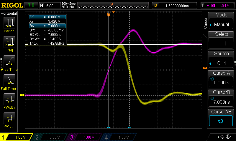 Oscilloscope trace of the inverter with wires of about the same length
This time you can see it’s much closer to the expected with a value of about 7 ns (2% out). So the simulation did a good job here.
Timing analysis
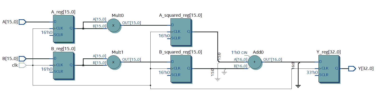
The next thing to go onto is timing analysis and something called timing closure. Combinational logic (that is logic that has no memory and only depends on the current input for its output) as we have seen has a propagation delay and doesn’t happen instantaneously. The more logic you have concatenated together the greater this propagation delay becomes. If this delay becomes too big the design won’t work. Let’s do an example, this time something that calculates the sum of two squares, i.e. (Pythagoras’s formula).
Create a new project and add the following as the top level Verilog file…
module sum_of_squares
#(
parameter N=16
)
(
input 			clk,
input  [N-1:0]		A,
input  [N-1:0]		B,
output [2*N:0]		Y
);

reg [N-1:0]		A_reg;
reg [N-1:0]		B_reg;
reg [2*N:0]		Y_reg;

//output wire is connected to the output reg
assign Y=Y_reg;

//flip flop the data into the holding regs
always @(posedge clk)
begin
A_reg<=A;
B_reg<=B;
end

//flip flop the result into the storage reg
always @(posedge clk)
begin
Y_reg<=(A_reg*A_reg+B_reg*B_reg);
end
endmodule
This describes hardware that has some combinatorial logic sandwiched between two flip-flops. You can see this from the netlist viewers → RTL viewer after you have done pin assignment and compiled the design…
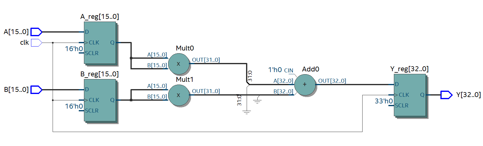 RTL view of the design
The clk pin synchronizes the movement of the data through the device. The first clock transition loads the A and B data into the combinatorial logic (Mult0, Mult1 and Add0) and at the same time outputs the previous result from the combinatorial logic to port Y. We require the combinatorial logic to calculate the result within one clock cycle else the design is not going to work. Let’s say we want to calculate the sum of squares 111 million times a second; that’s a clock speed of 111MHz.
Initially I was hoping that the multiplication would produce a large combinatorial delay for learning purposes so that timing closure would fail. However, if you look at the flow summary the compiler was clever and used hardware on the FPGA that is dedicated for multiplication. This can be seen in the following figure where it used 4 of the embedded multipliers...
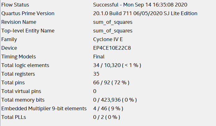 Flow summary of the design
If you’re interested you can see all the little logic elements, registers and multipliers used…
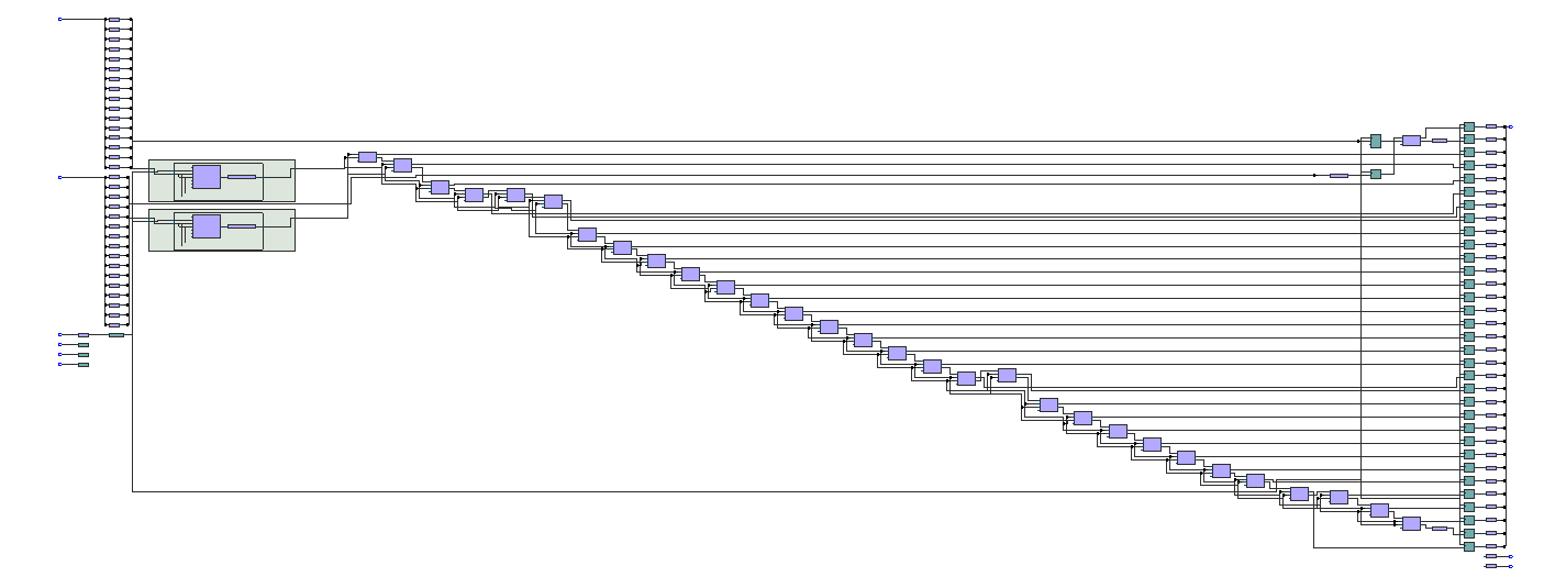 Gate level view of the design
You can see even for a simple design there are quite a lot of them.
Next go to tools → timing analyzer. Then double-click on “create timing netlist”…
 Timing analyzer
This seems a really complicated thing, but surely the most important thing to tell this tool is the input clock speed. So go to constraints → create clock. Call "clock name" clk and give "period" 9 ns (about 111MHz)…
 Create base clock
Click on the "…" next to targets, then "list", "find clock" then move it over to the right pane…
 Select clk as target
Then click OK then run. I believe what we’ve just done is called creating a constraint for the clock.
It seems to also be important to constrain the input and output ports, this is done with constraints → set input delay and constraints → set output delay. These input and output delays are dependent on what the FPGA is connected to. I am going to pretend I’m connecting the FPGA to 74ALVC74 flip-flops. Firstly let’s just set the input and output delay constraints for connecting the FPGA to 74ALVC74 flip-flops chips. Later I’ll explain how I derived these values from the 74ALVC74 data sheet.
Goto constraints → set input delay, set clock name “clk”, input delay “minimum”, 1ns delay value and for targets I’m adding A and B ports…
 Set minimum input delay
Then click run.
Do the same again except this time choose “maximum” with a delay value of 4.2ns.
Likewise do the same thing for constraints → set output delay except for the targets choose the Y port with the minimum delay of -0.7 ns and a maximum output delay of 0.9 ns.
Then click constraints → write SDC file. Click the "…" , remove the “.out” part of the file name from the dialog, and then save in the project’s directory (where your Verilog top level file lives)…
 Save the SDC file
This SDC file contains constraints and if you look at it, it should basically contain something equivalent to the following…
set_time_format -unit ns -decimal_places 3
create_clock -name {clk} -period 9.000 -waveform { 0.000 4.50 } [get_ports {clk}]
set_input_delay -add_delay -max -clock [get_clocks {clk}]  4.20 [get_ports {A[*] B[*]}]
set_input_delay -add_delay -min -clock [get_clocks {clk}]  1.00 [get_ports {A[*] B[*]}]
set_output_delay -add_delay -max -clock [get_clocks {clk}]  0.9 [get_ports {Y[*]}]
set_output_delay -add_delay -min -clock [get_clocks {clk}]  -0.7 [get_ports {Y[*]}]
I found after a while it was easier working with the SDC file directly than using the GUI interface. However the GUI interface was very handy for figuring out what commands were and how to use them.
Now the next time you start the timing analyzer you have to double click "update timing netlist". I’m not sure what all the reports are but double-clicking on “report clocks” should tell you “clk” is running at about 111 MHz…
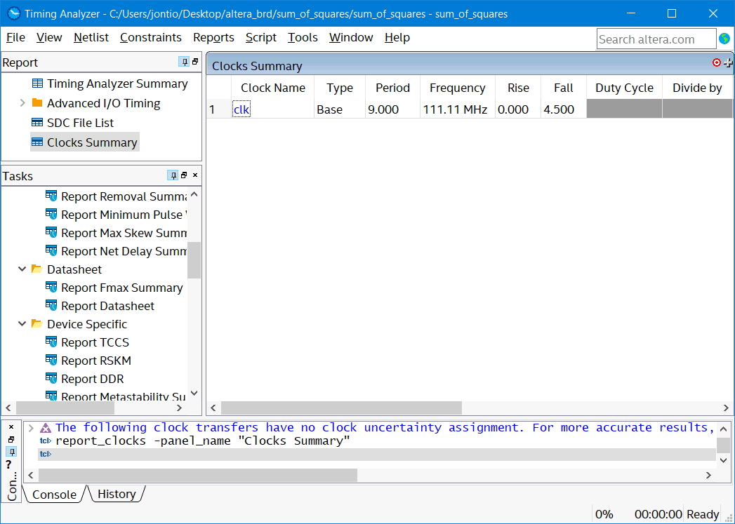 Clock summary
“Report Fmax summary” seems interesting and seems to tell you the maximum speed at which you can run your device…
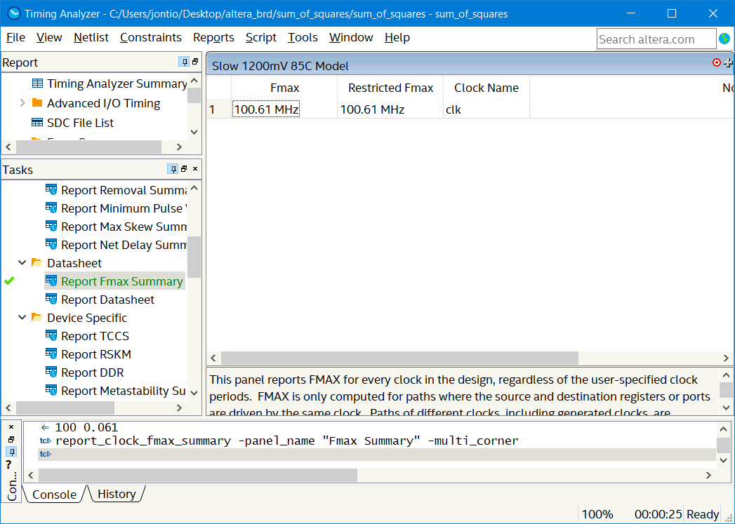 Fmax
Fmax
This means our design should fail as it is less than the 111 MHz we are running the clock at.
“Report unconstrained parts” seems to be important and if things are not zero then you need to set up timing analyzer a bit more; in my case they are all zero now.
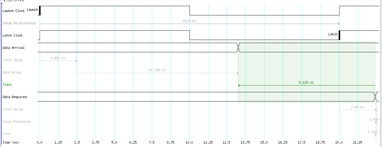
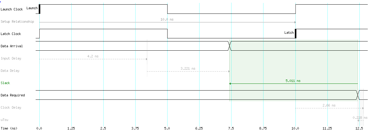
Something called slack is also important and negative numbers are bad while positive numbers are good. Slack tells you the amount of time in nanoseconds before things fail. For example if I double-click on “report timing” and click “report timing” I get the following figure. By default this runs setup time analysis which refers to time before data is required, the worst pathways appear at the top of the summary of pathways list by default…
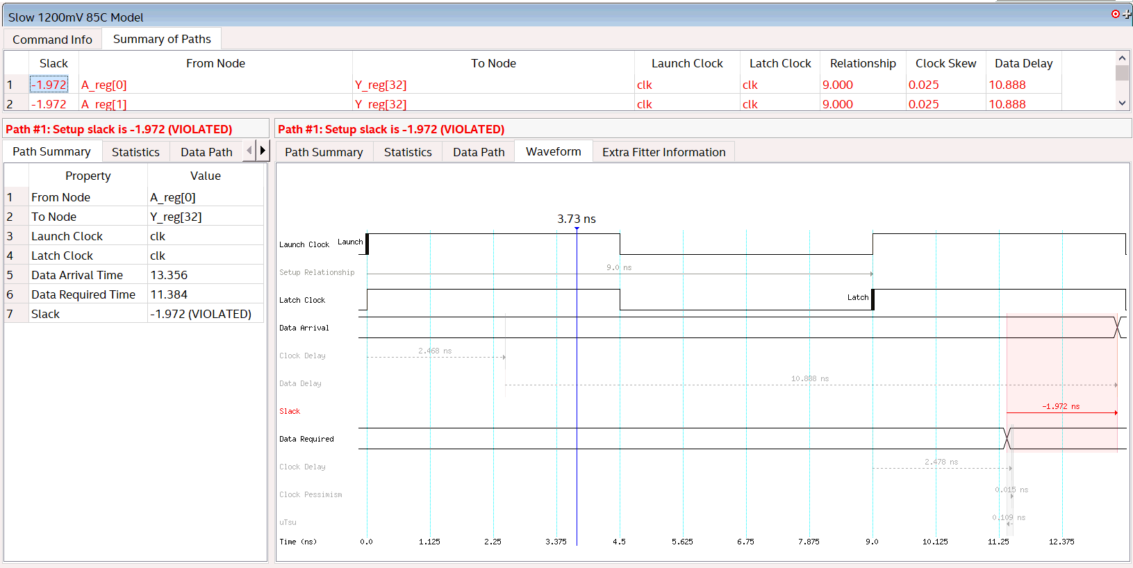 Paths failing timing
This means that data is not getting from A_reg to Y_reg quick enough. We either have to change our design or slow the clock down to below Fmax.
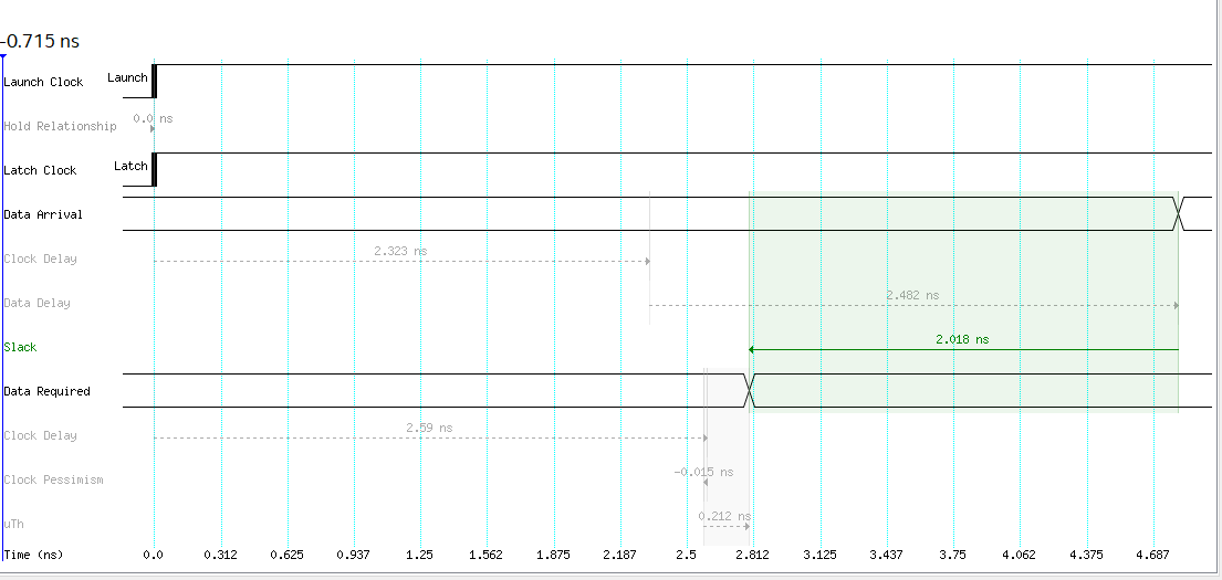
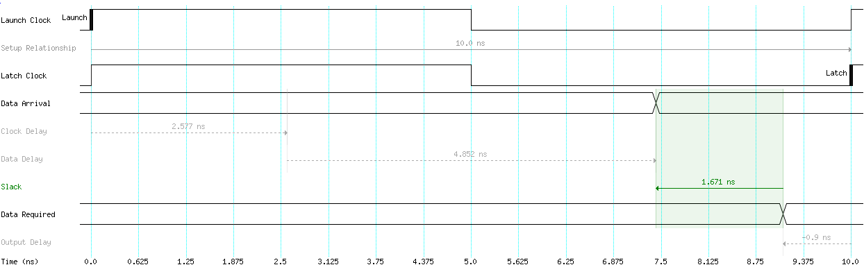
For setup analysis data arrival has to be before data required…
 Good setup analysis example
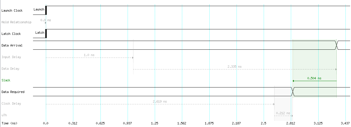
For hold analysis data arrival has to be after data required…
 Good hold analysis example
The launch clock is the clock to the input flip-flop while the latch clock is the one to the output flip-flop.
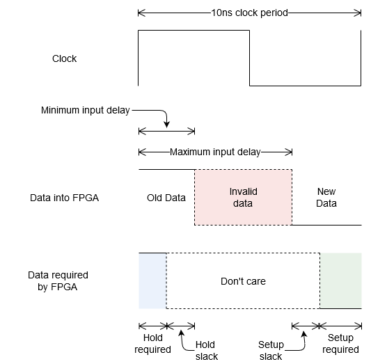
The setup and hold times refer to the time before and after the latch clock transition as can be seen in the figure below…
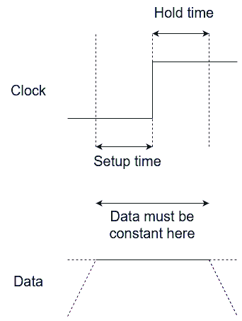 Setup and hold
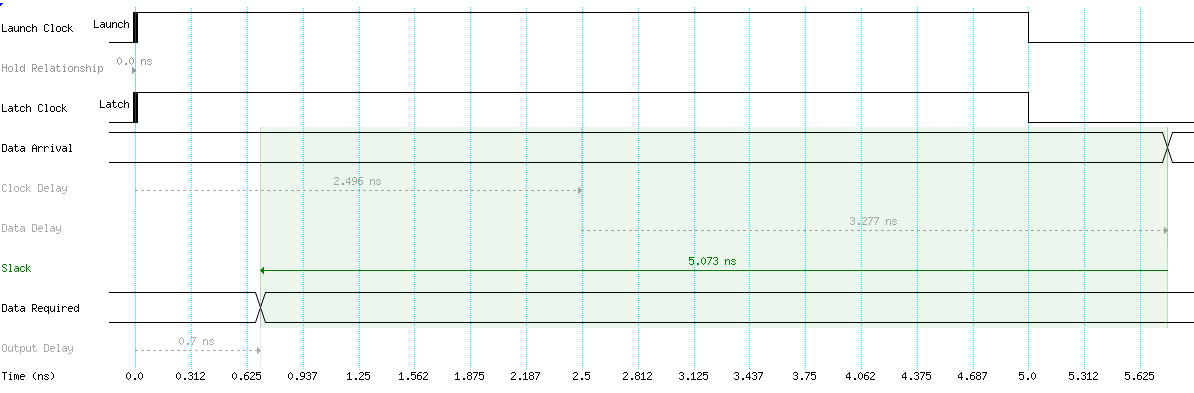
However, for the two previous good analysis plots the data required seems to be skewed about 2.5 ns by something called clock delay which I think is why the latch clock transitions are not where I would’ve expected to see them.
Double-clicking on "summary setup" then on "summary hold" both Slow 85C model I get the following for setup and hold respectively for 111MHz…
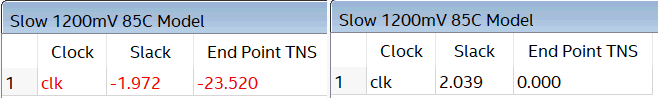 Setup and hold slacks
This seems to be the easiest thing to click on to see whether or not your design will work. So at 111MHz it’s failing on the setup requirements but it’s meeting the hold requirements. So we have to fix this problem.
Anyway, rather than slowing the clock down we can do something called pipelining which allows a speed increase at the expense of latency. Pipelining is like a production line where a factory full of workers that produce cars don’t just make one car before making the next car but rather make many cars simultaneously that are all in different stages. This means that none of the workers are waiting on previous workers to finish. For us this effectively means putting some flip-flops within the combinatorial section as can be seen in the following figure…
 Pipelined version of the design
These new flip-flops A_squared_reg and B_squared_reg cause Mult0 and Mult1 to work on a newer calculation than Add0 which works on the previous calculation with respect to Mult0 and Mult1. This doesn’t decrease throughput but on the downside it does increase latency by one clock cycle. This new design can be described in Verilog as follows…
module sum_of_squares
#(
	parameter N=16
)
(
	input 				clk,
	input  [N-1:0]		A,
	input  [N-1:0]		B,
	output [2*N:0]		Y
);

reg [N-1:0]		A_reg;
reg [N-1:0]		B_reg;
reg [2*N:0]		Y_reg;

//output wire is connected to the output reg
assign Y=Y_reg;

//flip flop the data into the holding regs
always @(posedge clk)
begin
	A_reg<=A;
	B_reg<=B;
end

//square the holding regs
reg [2*N-1:0]		A_squared_reg;
reg [2*N-1:0]		B_squared_reg;
always @(posedge clk)
begin
	A_squared_reg<=A_reg*A_reg;
	B_squared_reg<=B_reg*B_reg;
end

//add the squared regs together
always @(posedge clk)
begin
	Y_reg<=A_squared_reg+B_squared_reg;
end

endmodule
All the “always @(posedge clk)” blocks happen at the same time and as what’s in them is all nonblocking assignment I could have just written one block like the following but it would’ve been a bit more confusing I think…
reg [N-1:0]		A_squared_reg;
reg [N-1:0]		B_squared_reg;
always @(posedge clk)
begin
	B_reg<=B;
	A_squared_reg<=A_reg*A_reg;
	Y_reg<=A_squared_reg+B_squared_reg;
	B_squared_reg<=B_reg*B_reg;
	A_reg<=A;
end
Anyway time to run timing analysis again. This time Fmax is 120MHz…
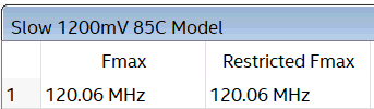 Fmax for pipelined version
For a clock speed of 111 MHz this produces the following setup and hold slack respectively…
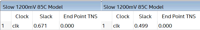 Setup and hold for pipelined version
This means our design should now work at 111 MHz.
The following figure shows a gate level simulation running at 111 MHz. There are three markers, one at positive clock transition, one 0.9ns before that market representing the setup period, and one 0.7ns after the positive clock transition representing the hold period. The period of time between the first market in the last marker is where the data must remain constant for the flip-flop to latch the incoming data from the FPGA. As you can see Y doesn’t change in this period so the output constraints have been met. The input constraints have also been met but I did not bother to show that here.
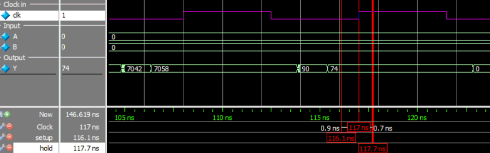 Gate level simulation for pipelined version
Anyway time to explain the input and output constraints and how I used the 74ALVC74 data sheet to drive them.
Getting my head around input and output constraints required for timing analysis was a bit tricky. It’s something that seems to be asked a lot but good information about it seems to be hard to come by. So far Xilinx’s ultrafast design methodology guide ug949 I have found to be the most helpful. They seem to update this document and I have noticed a 2015, 2016 and the 2020 version; there are probably more of them.
Set output delay
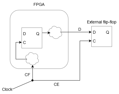
Let’s start with connecting an external device to the FPGA and the data travels from the FPGA to the external device. For this we have to set the output delay constraint in the constraint menu. Let’s say the external device is a flip-flop imagine and we have the following set up…
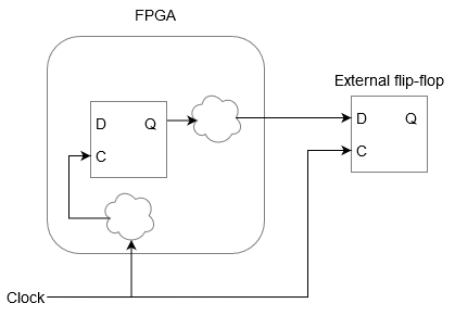 Data traveling from FPGA to an external flip-flop
There is an external clock that is clocking both the FPGA and the external flip-flop. Let’s ignore delays outside either the external flip-flop or the FPGA. Say the clock is working at 100 MHz. There are some delays inside the FPGA both on the clock pin and the data output pin but there is a flip-flop inside the FPGA that causes the data to emerge from the FPGA when the clock transitions from a low to a high.
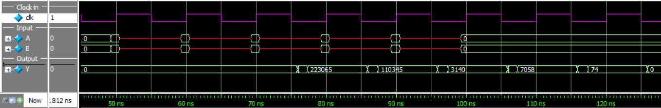
During one clock cycle there is some period of it that contains invalid data that the FPGA produces on the output data pin that the external device must ignore. This can be seen in the following gate level simulation of the FPGA outputting data where a number is changing from 110345 to 3140. There is a period of 1.569 ns where the data is changing and invalid data appears. In this case the invalid number 35908 is obvious but if you zoom in there are more invalid numbers that last for very short periods of time.
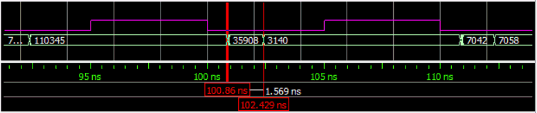 1.569 ns of invalid data
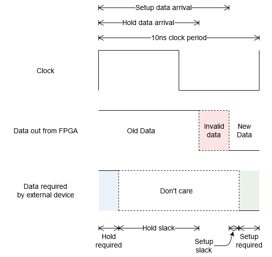
In the timing analysis tool when performing report timing for setup and hold you will see in the figures something called data arrival time. When doing report timing for hold this data arrival time (let’s call it hold data arrival) is the period of time from positive clock transition to when the invalid data begins. When doing report timing for setup this data arrival time (let’s call it setup data arrival) is the period of time from the positive clock transition to when the data becomes invalid then becomes valid again. So as long as our external flip-flop doesn’t require constant data during this invalid period our external flip-flop will capture the data from the FPGA. The following figure shows the clock, the data that comes out of the FPGA and the times when the external device does not want the data to change.
 Data from FPGA to an external device
For the external flip-flop the setup required is the period of time data must be constant before the positive clock transition while hold required period of time data must be constant after the positive clock transition. Slack tells you what your margin is before you end up requiring data in the invalid data region which means your system most likely won’t work, positive slack is good negative slack is bad.
For timing analysis minimum input and output delays are used for hold analysis while maximum input and output delays are used for setup analysis.
For output the hold required is the additive inverse of the minimum input delay while setup required is the maximum input delay. That’s a fancy way of saying the following two formulas.
Relationship between output delays and hold and setup requirements
Say we use the flip-flop 74ALVC74. This flip-flop is fast enough to do a couple hundred megahertz. Say we run this device at 2.7 V (I do this so the hold and setup times are different to make things clear). At this voltage the hold requirement () is less than 0.7ns and the setup requirement () is less than 0.9ns. Therefore I am going to set minimum and maximum output delays to the following…
Settings in timing analyzer for 74ALVC74 at 2.7V
To enter this data either use the menu constraints → set output delay or enter it manually into the SDC file as…
set_output_delay -add_delay -max -clock [get_clocks {clk}]  0.9 [get_ports {Y[*]}]
set_output_delay -add_delay -min -clock [get_clocks {clk}]  -0.7 [get_ports {Y[*]}]
Here are all my output ports are Y[0] … Y[32] and the clock is called “clk”. You also have to have set the clock constraint using the menu constraints → create clock or enter into the SDC file as…
create_clock -name {clk} -period 10.000 -waveform { 0.000 5.00 } [get_ports {clk}]
After that I run the following timing reports first for hold analysis and then setup analysis…
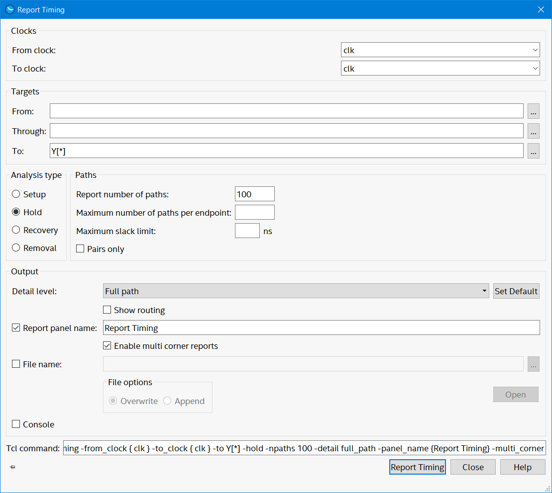 Create hold timing report for Y[*]
 Hold analysis of output pin with worst hold slack
You can see the output delay from this figure is 0.7 ns after the latch edge, this is the hold required I entered. While in this figure it’s called data arrival I think it should rather be called data exit as the data up until about five and half nanoseconds is the data you want and is good throughout this period.
 Setup analysis of output pin with worst setup slack
You can see the output delay in this figure is 0.9ns before the latch edge, this is the setup required I entered. I don’t have as much setup slack is the hold slack and the maximum setup required I could have had would have been about 2.5 ns.
From both of these figures if we subtract the set up data arrival time by the hold data arrival time we can calculate the period of time that data is invalid, in this case (4.852+2.577)-(3.277+2.496)=1.656ns. As I used the worst pins for both the setup and hold analysis any actual value should be less than or equal to this value. From the simulation I did previously you can see I got 1.569ns of invalid data which is around about the same value and less as expected. If you look at the simulation the invalid data started at 5.86 ns after the positive transition of the clock, this can be seen from the hold analysis plot where the clock delay plus the data delay is equal to 2.496+3.277=5.773ns which is about the same value and slightly less as this too is a worst case scenario. Anyway from these hold analysis and setup analysis plots you should be able to figure out where the invalid data appears in the clock cycle and how large it is.
Finally for the output delay if you want to model things a bit more accurately you can add the delays caused by the wires between the external flip-flop, the FPGA board and the clock as follows.
More precise relationship between output delays and hold and setup requirements
and is the hold and setup required respectively for the external flip-flop. , and are the delays caused due to the board traces for the data line, the clock to the FPGA and the clock to the external flip-flop respectively. The subscripts of and mean minimum and maximum values of these that you are likely to find respectively.
 Data traveling from FPGA to an external flip-flop taking into account external wires.
Anyway I’m not going to concern myself with the board traced delays just yet.
Set input delay
For this one data is traveling from the output of external flip-flop to the FPGA. Let’s imagine the following set up.
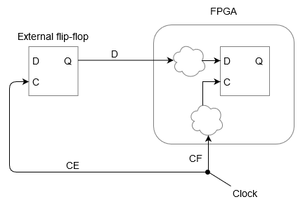 Data traveling from an external flip-flop to an FPGA.
This time the minimum and maximum delays (input delays this time) tell the FPGA when the data from the external flip-flop is invalid and to avoid sampling at this period. An input delay is the period of time between positive clock transition and the data arriving at the FPGA input data pin. The minimum delay is when the data starts changing and the maximum delay is when the data finishes changing. Therefore the period of time between these two delays the data is invalid. Again for simplicity we ignore the board delays , and .
 Data from external device to the FPGA
In the data sheet of the flip-flop this input delay to the FPGA is the propagation delay of the external flip-flop and is sometimes called . However in the data sheet I am looking at it’s called . For the 74ALVC at 2.7V it ranges from 1.0 ns to 4.2 ns. So that’s what we set the minimum and maximum input delays to. If we include the board trace delays we can model things a little more precisely with the following formulas.
More precise relationship between input delays and propagation delays
The setup and hold analysis figures for the worst input pins can be seen in the following figures…
 Setup analysis
 Hold analysis
You can see the minimum input delay has been used for the hold analysis while the maximum input delay is been used for setup analysis. If we increase the maximum input delay by the setup slack and decrease the minimum input delay by the hold slack, then this should create the largest period of invalid data possible and the design should only just work. That would mean a minimum input delay of 0.496 ns and a maximum input delay of 9.211 ns. As we have a clock period of 10 ns, valid data has to be present 0.789 ns before the positive clock edge (setup period) and 0.496 ns after the positive clock edge (hold period). Writing a test bench to contain valid data only during this period produced the following gate level simulation…
 Input data only valid when required
A and B are the input busses to the FPGA while Y is an output bus. The red lines signify invalid data input. The FPGA is performing a sum of squares so . Although you can’t see it in this screenshot the five numbers that come out from Y are correct and appear three clock cycles after A and B have been latched into the FPGAs flip-flops. This is the minimum period where A and B have to be constant. Yes I tried decreasing the setup period and the hold period, the minimum values I could get were 0.637ns and 0.482ns respectively. Anything less than this value would cause invalid data to appear on the output port Y. So there is a slight discrepancy of 152 ps and 14 ps for these five test inputs. However, there could be a sequence of test inputs that could cause it to fail, with the slightly smaller set up and hold times of 0.637ns and 0.482ns respectively. Anyway that’s good enough for me for now.
Asynchronous inputs
OK we have the ability to connect the FPGA to flip-flops that have the same clock is the one on the FPGA. However, things such as LEDs, pushbuttons, and UARTs have timings that are not related to a clock that the FPGA has access to and are asynchronous. So we have a problem.
For asynchronous inputs there is no guarantee that the inputs are going to transition when the FPGA would like the inputs to change. This means the FPGA can experience timing violations which means it could be latching invalid data that propagates through the FPGA causing all sorts of terrible things to happen. Latching of invalid data can cause pins to go into a metastable state not quite a one and not quite a zero. However, I believe flip-flops with metastable outputs eventually settle to a one or zero, it just takes a bit of time. A simple way to buy this time while the flip-flops are deciding whether or not there are a one or a zero is to concatenate a bunch of flip-flops together which create something called a synchronizer. This means the output of the synchronizer is less likely to be in a metastable state when it’s time to latch its value. Apparently there’s something called mean time between failures (MTBF) that you can calculate when creating these synchronizes but I have no idea how to do that at the moment. From what I read most people just add a couple of flip-flops together, say the meta-stability issue is solved and call it a day. Anyway, that’s more than enough to get going, the following figure is the traditional synchronizer and it’s only useful for one bit.
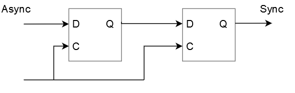 One bit synchronizer
It takes to clock cycles for the data to work its way through this synchronizer. Hopefully the extra clock cycle will be enough for the first flip-flop to settle down so that the output from the second flip-flop is synchronous with the FPGA’s clock. This doesn’t work for more than one bit such as buses but as we are thinking about a UART isn’t an issue for us yet.
For asynchronous inputs and Quartus it seems that you can define the input pin to the first flip-flop that it encounters as a false path so that it doesn’t complain about an unconstrained input. This can be done in timing analyzer. The easiest way I have found is by double-clicking on “report unconstrained parts”, “setup analysis”, “unconstrained input port paths”, right click the path and then left click “set false path”.
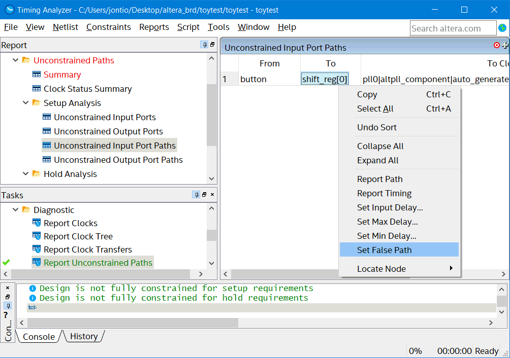 Setting a false path
In this example it adds “set_false_path -from [get_ports {button}] -to [get_keepers {shift_reg[0]}]” to the SDC file. Setting this is a false path means the compiler doesn’t worry about trying to meet any timing requirement for this path. However, I am wondering if using false paths is somewhat like chopping one’s fingernails with an axe and might not always be a good idea. For the time being however I’ll use false path for asynchronous inputs.
This input that I have called “button” is attached to a bunch of flip-flops. In the RTL viewer this circuit looks like the following…
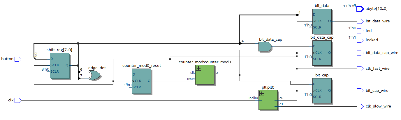 RTL viewer with a synchronizer
There are bits and pieces of other things thrown into the circuit as I’ve been experimenting with things but the synchronizer is comprised of shift_reg[7..0]. It looks different from the previous figure but if your flip-flops are suffixed with numbers then RTL viewer draws them in the strange compact way. Anyway, if we feed in some asynchronous stimulus to “button” we should always get valid data on “bit_data_wire” in a gate level simulation right? Nope!!!
First off some asynchronous data I created with the following test bench…
`timescale 1ps/1ps

module toytest_tb;

reg clk;
reg button;

localparam PERIOD=20000;

toytest toy0
(
	 .clk(clk),
	 .button(button)
);

integer i;
initial
begin
	clk=0;
	for(i=0;i<2*40*100;i=i+1)
	begin
		#(PERIOD/2);
		clk=~clk;
	end
end

integer k;
initial
begin
	for(k=0;k<100;k=k+1)
	begin
		#(4*PERIOD+100*k);
		button=0;
		#(6*PERIOD);
		button=1;
		#(12*PERIOD);
		button=0;
		#(1*PERIOD);
		button=1;
		#(1*PERIOD);
		button=0;
		#(1*PERIOD);
		button=1;
		#(1*PERIOD);
		button=1;
		#(1*PERIOD);
		button=0;
		#(1*PERIOD);
		button=1;
		#(1*PERIOD);
	end
end

endmodule
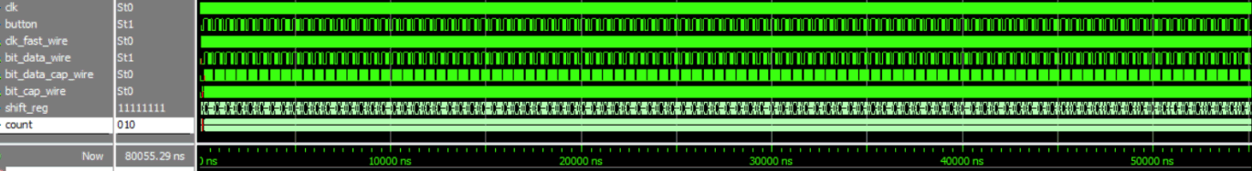
It sends out a series of pulses to “button” whereby it shifts the phase by 100ps each iteration. Shifting it by 100ps each iteration means I can test to see if the circuit performs as desired under different situations. The following figure shows some of the output of this test when running a gate level simulation…
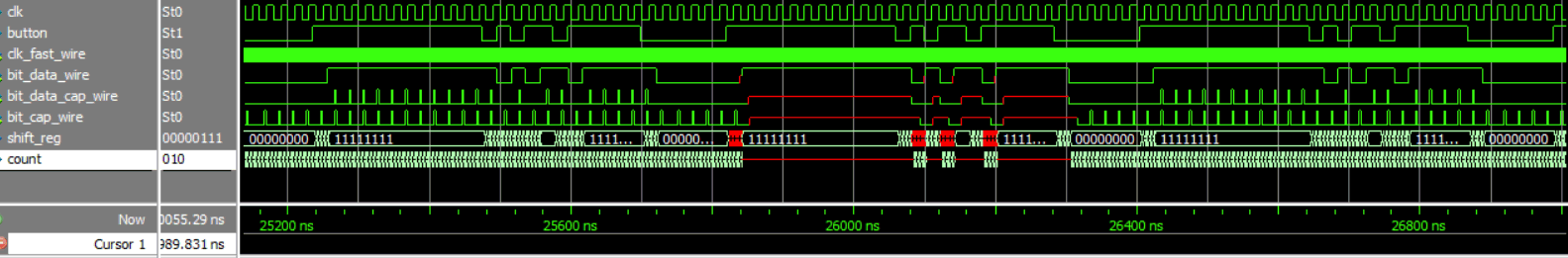 Gate level simulation with a synchronizer but showing expected results
As can be seen in this figure there are bits of various signal wires that are colored red. There are small periods of time where “bit_data_wire” is red, but these small red periods propagate into the “count” register and others causing much more significant redness. The red color means an undefined value in ModelSim. If we look more closely at the synchronizer “shift_reg” we can see how the undefined value propagates into the system…
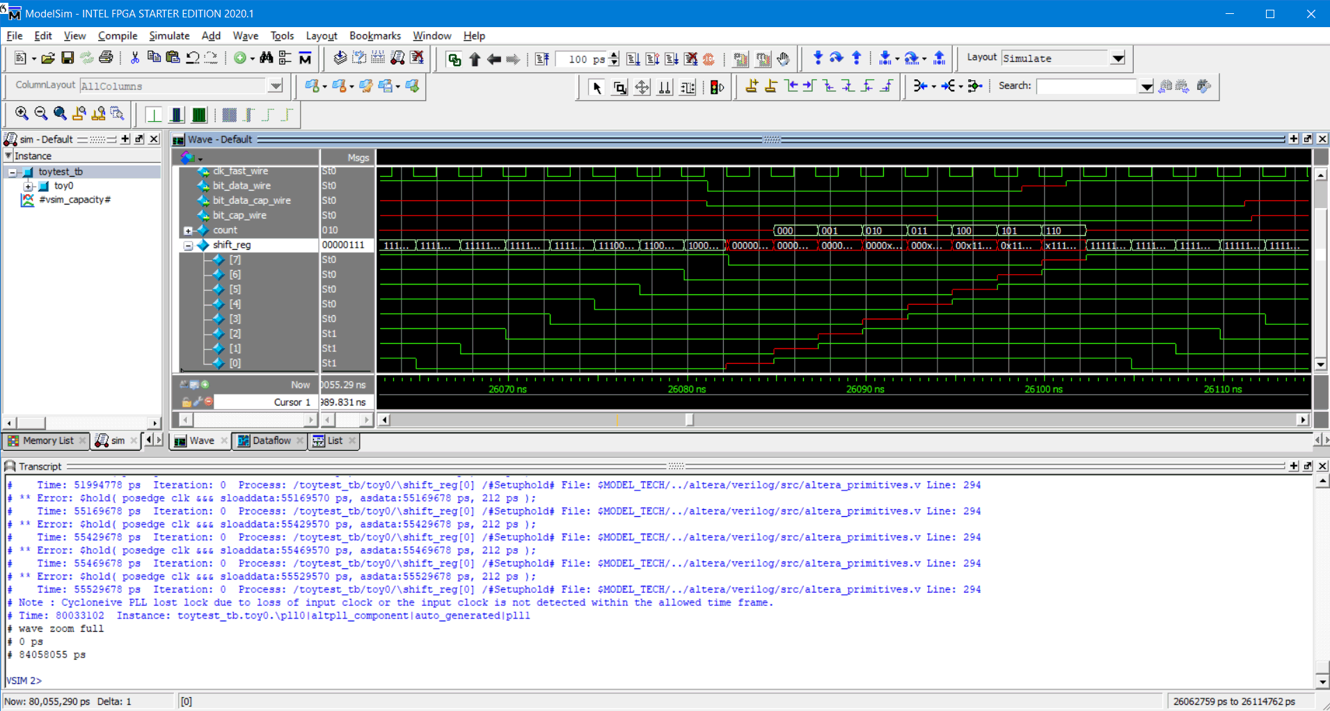 Undefined value shifting through system
As can be seen the undefined value propagates from shift_reg[0] then goes into shift_reg[1] and so on; this is not expected. The whole idea of the synchronizer is that if the shift_reg[0] flip-flop was to capture invalid data by the time it got to shift_reg[7] it should’ve become a one or zero. So with a bit of head scratching I managed to stumble across https://groups.google.com/g/comp.lang.verilog/c/tarsr7WXURE where someone was asking what to do for this annoying problem. "tcheck_set" was mentioned but I’m not sure what that’s about or where you enter that, SDF files were mentioned but those files don’t seem to exist for Quartus but SDO files do which I think of the same but I don’t really know how to modify the manually and even if I did that would be changed by Quartus every time I recompiled. Making a custom flip-flop was mentioned which might be a viable solution but I’ve yet to investigate how to do this. However, starting vsim with the option "+no_notifier" was mentioned if I had no desire to know about setup and hold violations; this seemed to be the easiest I just had to remember that setup and hold violations would be missed in simulation so I would have to be careful to pick them up in timing analyzer.
So the next problem how to start vim with "+no_notifier"? Looking in Quartus I couldn’t find any way of modifying the commands it sent to ModelSim when pressing the “gate level simulation” button. When you press this button it seems to create a file called “toytest_run_msim_gate_verilog.do” for my example which contains the commands it seeds to ModelSim. For me I see the following things and that file…
transcript on
if {[file exists gate_work]} {
	vdel -lib gate_work -all
}
vlib gate_work
vmap work gate_work

vlog -vlog01compat -work work +incdir+. {toytest_8_1200mv_85c_slow.vo}

vlog -vlog01compat -work work +incdir+C:/Users/jontio/Desktop/altera_brd/toytest {C:/Users/jontio/Desktop/altera_brd/toytest/toytest_tb.v}

vsim -t 1ps +transport_int_delays +transport_path_delays -L altera_ver -L cycloneive_ver -L gate_work -L work -voptargs="+acc"  toytest_tb

do C:/Users/jontio/Desktop/altera_brd/toytest/simdo.do
The last line in that file runs my script which I can control. The line above that one is the one I wish to add the "+no_notifier" option to but I can’t as if I modify that file again Quartus will delete my changes every time I run a gate level simulation. So although not particularly tidy and adds extra time as the vsim command has to run twice but the solution I went for was to copy that vsim command and paste the modified version of it into my simdo.do file. The following is my modified simdo.do file…
vsim  +no_notifier +transport_int_delays +transport_path_delays -L altera_ver -L cycloneive_ver -L gate_work -L work -voptargs="+acc"  toytest_tb
add wave -position end sim:/toytest_tb/toy0/*
run -all
wave zoom full
It’s a bit crazy but I’m not sure what other way to do it. Anyway saving the simdo.do file and running gate level simulation again I get the following…
 Gate level simulation with a synchronizer showing expected results
Now the only red there is, is during the initial startup which is not due to timing violations but instead due to a long period of time where “button” set to an undefined value which I did on purpose. This will do for the meantime for asynchronous inputs and should be enough to allow me to create the receiving side of a UART.
Designing the UART RX overview
I have already created one UART that worked in real life at 50 Mb per second. However, running timing analysis said it shouldn’t work. Initially I just designed the UART for slow speeds between the computer and the FPGA board and in that case both simulation and real life testing agree and say it should work. The following figure shows the design of this first UART receiver.
 Slow RX UART schematic
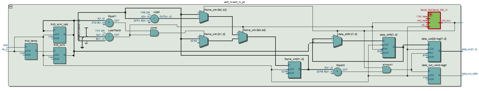
There is not much to it, some flip-flops on the input and the output with mostly a whole bunch of combinatorial stuff in the middle. The baud bit tick generator module that you see in it creates the bit strobe for the incoming data. It doesn’t have any exact oversampling requirement per se but I would suggest at least eight times oversampling would be about the minimum. So if that’s the case then that’s 400 MHz for 50Mb/s UART. Performing some simulations I got an Fmax of around 170 MHz. That’s fine for 5Mb/s but not for 50 Mb/s. Why it worked in real life at 50 Mb/s? I’m not sure. So let’s throw out that design and start again. The figure below shows the design I have in mind for the receiving side of the 50Mb/s UART.
 Fast RX UART schematic
This time I’m planning on two synchronized clocks produced by one of the phase locked loop’s inside the FPGA. One of the clocks will be that of the desired baud rate and the other one will be eight times that speed for sampling the rx serial line. The incoming synchronizer will also be used as a delay line so that I can both detect the falling edge of the start bit as well as sampling the rx line at the optimal moment. I’ll then use two counters. The first counter “counter_strobe” will output a strobe on every eighth sample, while the second one “counter_timeout” will disable detecting a start bit transition for 9.5 bits by producing an “idle” line. The second timer will also produce a “convert” line that can be used to identify when a byte starts. The bits that are sampled at the optimal time using the fast clock are then stored in a register “bit_data_latched”. During the conversion from serial to parallel the output of “bit_data_latched” will be updated once every 8 fast clock cycles or equivalently every 1 slow clock cycles and will happen synchronously with respect to each clocks. Finally a serial to parallel converter will package up the eight consecutive bits once it is told the bits are starting via the “convert” line. All the modules used should have lots of pipelining and output registers.
This time with simulations I got an Fmax around 450 MHz for the fast clock with a setup slack around the 0.4ns mark. Although it’s supposed to be run with 400 MHz for the fast clock and 50 MHz for the slow clock I reduced these clocks to produce a 115200 b/s baud rate. Running an RTL simulation test bench with some input data on the rx line I produced the following figure of the wires inside the rx UART.
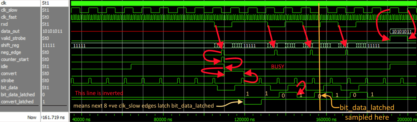 RTL simulation of the fast RX UART
Testing the fast rx UART design in real life with a slow input signal
I had already done lots of simulation by this time with both gate level and RTL so I wanted to test it out on real hardware. To do this, I added an LED segment display driver module that I had already created to display the “data_out”. This display driver module was one of the first things I wrote in Verilog. It contains a huge amount of combinatorial logic without many flip-flops at all. That’s fine as there are only eight LED segments on the development board that need refreshing at say 60 Hz. That means as long as everything can propagate through the combinatorial logic in 2 ms (480Hz for 8 segments) it should work. 2 ms is really slow and means propagation delay can almost be ignored. You might get some messed up output if the input changes rapidly but if that happens you won’t be able to read the display anyway. Also I’m creating a clock by dividing the main clock using flip-flops which I now know is bad. So just pretend you don’t see that. For timing analysis and timing analysis driven compilation I am setting anything that goes through the segment display module as a false path so as to inform the compiler not to bother about trying to meet any timing constraints for the segment display. I am also adding a false path to the asynchronous serial input to the design. The following are my false paths…
set_false_path -from [get_ports {rx_pc}] -to [get_keepers {uartrx:uartrx0|shift_reg[0]}]
set_false_path -to [get_ports {segData[*]}]
set_false_path -to [get_ports {segSelect[*]}]
I’m not too sure how to constrain the clock output from the clock divider so I set it as a generated clock but in retrospect I think I should have used “create clock” as I don’t know the phase relationship between the master clock in this new clock. Initially I use the following constraint…
create_generated_clock -name {segDisplay_clk} -source [get_ports {clk}] -divide_by 208333 -master_clock {clk} [get_keepers {clock_div:clock_div_seg0|clk_out}]
However that division is so large when it compiles I get the following notification…
“Warning (332007): The period, rise edge, or fall edge of clock: clock_div:clock_div_seg0|clk_out was found to be outside of the range of acceptable time values. The minimum acceptable time value is -2147483.647 and the maximum acceptable time value is 2147483.647. This clock will be ignored.”
From https://community.intel.com/t5/Intel-Quartus-Prime-Software/how-to-constrain-low-frequency-clocks/m-p/16798/highlight/true?profile.language=ko it seems for these very low frequencies you just lie. So I used the following one instead…
create_generated_clock -name {clock_div:clock_div_seg0|clk_out} -source [get_ports {clk}] -divide_by 2000 [get_keepers {clock_div:clock_div_seg0|clk_out}]
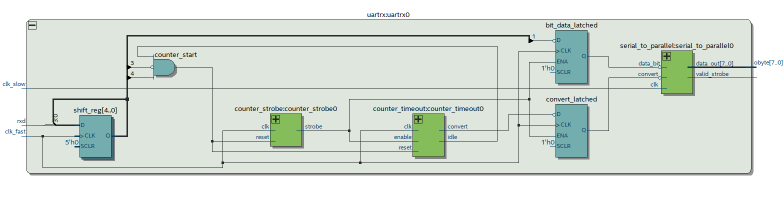
Anyway here’s the schematic with the main clock coming in, the PLL for the rx UART and the bad design for the stuff to display things on the LED segment display.
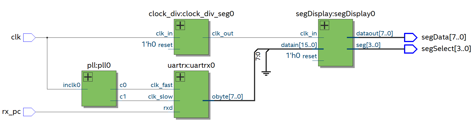 Top level module for real life RX UART test
The “clock_div” just divides the clock. The “segDisplay” drops leading zeros and converts the number from binary into binary coded decimal. The following shows the schematic for “segDisplay”, as you can see it’s huge.
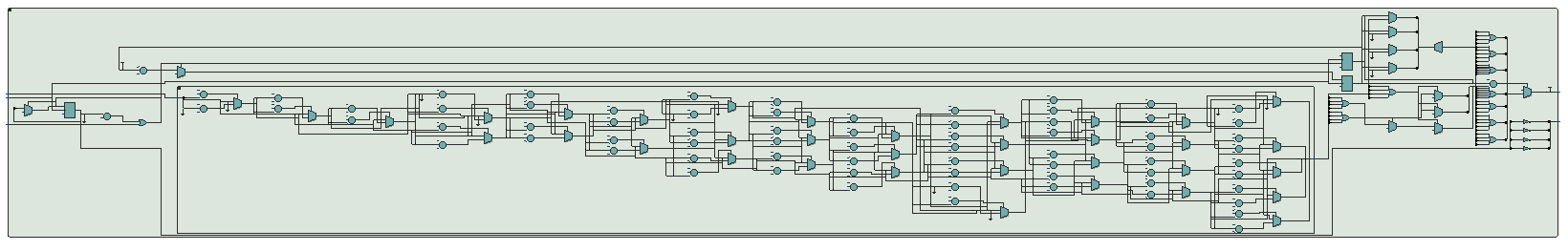 Segment display schematic
Most of its for the binary to decimal conversion which I copied from Wikipedia…
module bin2bcd
 #( parameter                W = 18)  // input width
  ( input      [W-1      :0] bin   ,  // binary
    output reg [W+(W-4)/3:0] bcd   ); // bcd {...,thousands,hundreds,tens,ones}

  integer i,j;

  always @(bin) begin
    for(i = 0; i <= W+(W-4)/3; i = i+1) bcd[i] = 0;     // initialize with zeros
    bcd[W-1:0] = bin;                                   // initialize with input vector
    for(i = 0; i <= W-4; i = i+1)                       // iterate on structure depth
      for(j = 0; j <= i/3; j = j+1)                     // iterate on structure width
        if (bcd[W-i+4*j -: 4] > 4)                      // if > 4
          bcd[W-i+4*j -: 4] = bcd[W-i+4*j -: 4] + 4'd3; // add 3
  end

endmodule
Anyway, I am not here to talk about the segment display driver but I just mention that I now have a way of visualizing the rx UART in real life.
The HDL (hardware description language) in Verilog for the top level module for the real life rx UART test is as follows...
module uartrxtest
#(
	parameter ClkFrequency = 50000000,//clk input
	parameter SEGS=4,
	parameter SEG_REFRESH_RATE=60 //60Hz
)
(
	input clk,//50MHz
	input rx_pc,//signal in
	output [7:0] segData,//LED seg data
	output [SEGS-1:0] segSelect//LED seg select
);

//pll for rx uart
wire clk_slow;//baud rate
wire clk_fast;//8*baud rate
pll pll0
(
	clk,
	clk_fast,
	clk_slow
);

//rx uart
wire [(4*SEGS)-1:0] obyte;//valid when ovalid is high but will not change till ovalid strobes again
wire ovalid;//high for 1 bit to mark a valid obyte
uartrx uartrx0
(
	.clk_slow(clk_slow),//baud rate
	.clk_fast(clk_fast),//8*baud rate
	.rxd(rx_pc),//signal in
	.obyte(obyte[7:0]),//valid when ovalid is high but will not change till ovalid strobes again
	.ovalid(ovalid)//high for 1 bit to mark a valid obyte
);

//slow display clock
wire segDisplay_clk;
clock_div
#(.DIVISOR(ClkFrequency/(SEGS*SEG_REFRESH_RATE)))//SEG_REFRESH_RATE Hz refresh
clock_div_seg0(.clk_in(clk),.reset(0),.clk_out(segDisplay_clk));

//display
segDisplay
#(
.SEGS(SEGS), //# of segs to use
.DROP_LEADING_ZEROS(1), // if set to 1 then leading zeros wont be displayed
.DIPLAY_AS_DEC(1) // if 1 then datain will be displayed as dec else will be displayed as hex
)
segDisplay0
(
	.clk_in(segDisplay_clk),
	.datain(obyte),
	.reset(1'b0),
	.dataout(segData),
	.seg(segSelect)
);
endmodule
The HDL for the rx UART module itself is as follows…
module uartrx
(
	input clk_slow,//baud rate
	input clk_fast,//8*baud rate
	input rxd,//signal in
	output [7:0] obyte,//valid when ovalid is high but will not change till ovalid strobes again
	output ovalid//high for 1 bit to mark a valid obyte
);

//sr for both delay line and syncronizer
parameter SHIFT_REG_LEN=5;
reg [SHIFT_REG_LEN-1:0] shift_reg=0;
always@(posedge clk_fast)
begin
	shift_reg<={shift_reg[SHIFT_REG_LEN-2:0],rxd};
end

//edge detect, counter and lockout
wire neg_edge;//neg edge detect
wire counter_start;//resets/starts the counters
wire idle;//if the line is idle
wire convert;//will go high when valid data arrives
wire Dclk;//data bit clock
wire bit_data;//data offset in future from bit edge
counter_strobe counter_strobe0(clk_fast,counter_start,Dclk);
counter_timeout counter_timeout0(clk_fast,Dclk,counter_start,idle,convert);
assign neg_edge=(shift_reg[SHIFT_REG_LEN-1] & ~shift_reg[SHIFT_REG_LEN-2]);
assign counter_start=(neg_edge&&idle);
assign bit_data=shift_reg[SHIFT_REG_LEN-4];//shift so we are looking at center of symbol rather than edge

//add flipflops to data and convert.
//the strange way of writing this was because
//this gave the best fmax and slack the compiler could
//do as well as making a readable RTL schematic
reg bit_data_latched;
reg convert_latched;
always @(posedge clk_fast)
begin
	if(Dclk)
	begin
		convert_latched<=~convert;
		bit_data_latched<=~bit_data;
	end
end

//convert to parallel
wire [7:0] latched_byte;
wire latched_byte_strobe;
serial_to_parallel #(.N(8)) serial_to_parallel0(clk_slow,(~convert_latched),(~bit_data_latched),latched_byte_strobe,latched_byte);

//for output port assignments
assign obyte=latched_byte;
assign ovalid=latched_byte_strobe;

endmodule

//---------------- submodules begin -------------------

module serial_to_parallel
#(parameter N=8)
(input clk,convert,data_bit,output reg valid_strobe, output reg [N-1:0] data_out);
reg act=0;
initial valid_strobe=0;
reg [N-1:0] abyte;
reg [$clog2(N)-1:0] counter=0;
always @(posedge clk)
begin
	valid_strobe<=0;
	act<=0;
	if(|counter)
	begin
		abyte<={data_bit,abyte[N-1:1]};
		counter<=counter-1;
		act<=1;
	end
	else if(act)
	begin
		valid_strobe<=1;
		data_out<=abyte;
	end
	else if(convert)
	begin
		counter<=(N-1);
		abyte<={data_bit,abyte[N-1:1]};
	end
end
endmodule

//next 2 modules take carefull note of resets. The resets
//must cause the state of the two counters to happen at
//the same time.

//strobe every 8 clks
module counter_strobe(input clk,reset,output reg strobe);
parameter N=3;
reg [N-1:0] count=0;
initial strobe=1;
always@(posedge clk)
begin
	if(reset)
	begin
		strobe<=0;
		count<=1;
	end
	else
	begin
		count<=count+1'b1;
		strobe<=!(|count);
	end
end
endmodule

//timeout after 8 enabled clks plus a bit (IDLE_HOLD_DELAY). timeout causes idle to go high.
//convert goes high on reset and will go low on next enabled clk. when it goes high it's
//time to convert the current 8 bits from serial to parallel
module counter_timeout(input clk,enable,reset,output reg idle,output reg convert);
reg invalid;
parameter N=3;
parameter IDLE_HOLD_DELAY=9;
reg [N-1:0] count=0;
reg [IDLE_HOLD_DELAY-1:0] shift_reg=0;
initial invalid=0;
initial idle=0;
always@(posedge clk)
begin
	{idle,shift_reg}<={shift_reg[IDLE_HOLD_DELAY-1:0],invalid};
	if(reset)
	begin
		{invalid,idle,count}<=0;
		shift_reg<=0;
		convert<=1;
	end
	else if(enable)
	begin
		count<=count+1'b1;
		if(&count)invalid<=1;
		convert<=0;
	end
end
endmodule
Compilation resulted in no timing errors. Loading the design into the FPGA everything seemed to work correctly as I pressed the buttons. The image below was the result after I pressed the “0” button on the computer which is 48 decimal in ASCII.
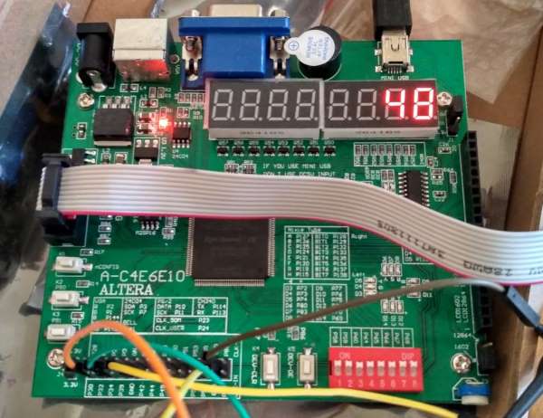 Pressing "0" on the computer produced the ASCII decimal representation 48 of it on the FPGA development board
Design validation by simulation
OK so it looks like it works when running slowly in real life. But does it work under all circumstances and also at higher speeds? That’s hard to say with real life tests, so simulation is extremely important and why so much talk on the Internet is about design validation by simulation. Let’s make a test bench to perform an RTL simulation for the design we have already put on the real life FPGA evaluation board.
This time I’ll try a little bit of SystemVerilog. SystemVerilog is an extension of Verilog and can be used for synthesis as well as simulation. It’s 100% backwards compatible with Verilog so I see no reason why not to use it instead of Verilog. He is the SystemVerilog test bench I put together to put some stimulus into the design and check that the design performs correctly for at least the things I’m interested in.
`timescale 1ps/1ps

module uartrxtest_tb;

localparam CLK_PERIOD=20000;//50MHz
localparam BIT_PERIOD=8680556;//115200b/s
localparam RANDOM_SEED_NUMBER=0;
localparam NUMBER_OF_TRIES=20;
localparam SENT_BIT_PERIOD_MAX_ERROR_IN_PERCENT=5;
localparam MAX_DELAY_BETWEEN_BYTES=(BIT_PERIOD*11);

//dut
logic clk;//50MHz
logic rx_pc;//signal in
uartrxtest dut(.*,.segData(),.segSelect());

//get wires from inside dut that we need
wire ovalid=dut.uartrx0.ovalid;
wire [7:0] obyte=dut.uartrx0.obyte;

//clock till we are told to stop
logic stop=0;
initial
begin
	clk=0;
	forever
	begin
		#(CLK_PERIOD/2);
		clk=~clk;
		if(stop)break;
	end
end

logic waiting_for_rx_byte=0;
logic [7:0] last_x;

//a task for simulating data from say the computer
task simulate_rx_byte(logic [7:0] x,int bitPeriod);
	if(stop)return;

	//send byte
	rx_pc=0;
	#(bitPeriod);
	for(int i=0;i<8;i++)
	begin
		rx_pc=x[i];
		#(bitPeriod);
	end
	rx_pc=1;
	#(bitPeriod);

	//check if waiting for rx byte
	if(waiting_for_rx_byte)
	begin
		$error("two simulated bytes sent and no rx byte from the first. failed to receive in time");
		stop=1;
		return;
	end

	last_x=x;
	waiting_for_rx_byte=1;
endtask

//check byte is received is the same as was was sent
always @(*)
begin
	if(waiting_for_rx_byte&&ovalid)
	begin
		waiting_for_rx_byte=0;
		if(obyte!=last_x)
		begin
			$error("rxed obyte not the same as the one that was sent (%d !=%d )",obyte,last_x);
			stop=1;
		end
	end
end

//send bytes to dut
logic [7:0] simulated_sent_number;
localparam BIT_PERIOD_MIN=BIT_PERIOD-(SENT_BIT_PERIOD_MAX_ERROR_IN_PERCENT*(BIT_PERIOD/100));
localparam BIT_PERIOD_STEP=2.0*(SENT_BIT_PERIOD_MAX_ERROR_IN_PERCENT*(BIT_PERIOD/100))/NUMBER_OF_TRIES;
real current_bit_period=BIT_PERIOD_MIN;
initial
begin
	//some time for things to start up
	rx_pc=1;
	#(BIT_PERIOD*12);

	$info("starting increasing bit periods from -%d%% to +%d%%",SENT_BIT_PERIOD_MAX_ERROR_IN_PERCENT,SENT_BIT_PERIOD_MAX_ERROR_IN_PERCENT);

	for(int k=0;k<NUMBER_OF_TRIES;k++)
	begin
		if(k==0)simulated_sent_number=$urandom(RANDOM_SEED_NUMBER);
		else simulated_sent_number=$urandom();
		simulate_rx_byte(simulated_sent_number,int'(current_bit_period));
		current_bit_period+=real'(BIT_PERIOD_STEP);
		if(stop)break;
	end

	$info("starting random bit periods");

	for(int k=0;k<NUMBER_OF_TRIES;k++)
	begin
		if(k==0)simulated_sent_number=$urandom(RANDOM_SEED_NUMBER);
		else simulated_sent_number=$urandom();
		current_bit_period=BIT_PERIOD-(SENT_BIT_PERIOD_MAX_ERROR_IN_PERCENT*(BIT_PERIOD/100))+($urandom%(SENT_BIT_PERIOD_MAX_ERROR_IN_PERCENT*2*(BIT_PERIOD/100)));
		simulate_rx_byte(simulated_sent_number,int'(current_bit_period));
		if(stop)break;
	end

	$info("starting random bit periods and random delays between sending bytes");

	for(int k=0;k<NUMBER_OF_TRIES;k++)
	begin
		if(k==0)simulated_sent_number=$urandom(RANDOM_SEED_NUMBER);
		else simulated_sent_number=$urandom();
		current_bit_period=BIT_PERIOD-(SENT_BIT_PERIOD_MAX_ERROR_IN_PERCENT*(BIT_PERIOD/100))+($urandom%(SENT_BIT_PERIOD_MAX_ERROR_IN_PERCENT*2*(BIT_PERIOD/100)));
		simulate_rx_byte(simulated_sent_number,int'(current_bit_period));
		if(stop)break;
		simulated_sent_number='x;
		#($urandom%MAX_DELAY_BETWEEN_BYTES);
	end

	//some time before stopping
	#(BIT_PERIOD*8);
	stop=1;

	//check if waiting for rx byte
	if(waiting_for_rx_byte)
	begin
		$error("failed to receive sent byte");
		stop=1;
	end

end

endmodule
I called this file uartrxtest_tb.sv added it to the testbed option in the EDA simulation tab like I described earlier. I then added the following simdo.do file also like I described earlier.
#add things from tb
add wave -position end -label "clk" sim:/uartrxtest_tb/clk
add wave -position end -label "rx_pc" sim:/uartrxtest_tb/rx_pc
add wave -position end -radix unsigned -label "simulated_sent_number" sim:/uartrxtest_tb/simulated_sent_number
add wave -position end -label "waiting_for_rx_byte" sim:/uartrxtest_tb/waiting_for_rx_byte
#add wave -position end -label "current_bit_period" sim:/uartrxtest_tb/current_bit_period
#this is for 115200 +-5%
add wave -position end -label "current_bit_period" -analog -min 8246530 -max 9114580 -height 30 sim:/uartrxtest_tb/current_bit_period

add wave -divider "uartrx0"

#add some uartrx0 items
add wave -position end -radix unsigned -label "obyte" sim:/uartrxtest_tb/dut/uartrx0/obyte
add wave -position end -label "ovalid" sim:/uartrxtest_tb/dut/uartrx0/ovalid
add wave -position end -label "clk_slow" sim:/uartrxtest_tb/dut/uartrx0/clk_slow

run -all
wave zoom full
Running the RTL simulation I got the following output from modelsim.
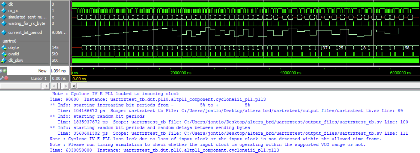 RTL simulation of RX UART
The test bench performs three tests. The first one it slowly increases the bit period making sure the random bytes that are simulated are decoded correctly by the design. The second test randomly changes the bit period for each byte that is simulated. The third test puts random delays between sending the simulated bytes. In all tests if bytes are incorrectly decoded or don’t turn up within time an error message is sent to the user and the simulation is stopped. However, as you can see from the figure the test bench ran to completion without any errors.
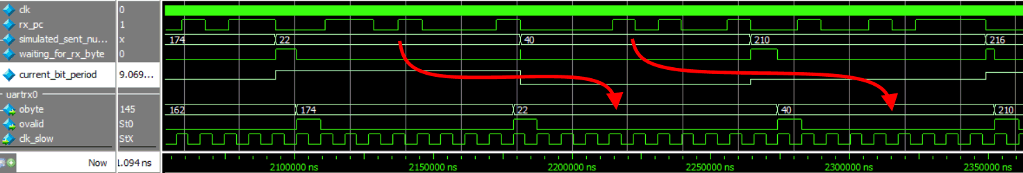
In the following close-up view you can see that when the bit period is larger than nominal the receiver decodes the incoming byte before it has finished. While when the bit period is smaller than nominal the next byte is being received before the previous one has even been decoded.
 Close-up of RX UART simulation
So it looks like design can cope with up to about a 5% bit rate error. That’s good; anything above about 1% is good.
So at 115200b/s we now we have something that passes timing analysis, an RTL test bench and seems to work in real life. We can’t test this device at 50 Mb per second in real life as the computer can’t output that speed. However, we can still simulate it. Changing the PLL to the 400MHz/50MHz output and running compilation again passed successfully without any timing violations. Changing the test bed parameters to the following…
localparam CLK_PERIOD=20000;//50MHz
localparam BIT_PERIOD=20000;//50Mb/s
localparam RANDOM_SEED_NUMBER=0;
localparam NUMBER_OF_TRIES=200;
localparam SENT_BIT_PERIOD_MAX_ERROR_IN_PERCENT=5;
localparam MAX_DELAY_BETWEEN_BYTES=(BIT_PERIOD*30);
…then running the RTL simulation resulted in receiving an erroneous byte when testing for random bit periods even though the past when doing increasing bit periods.
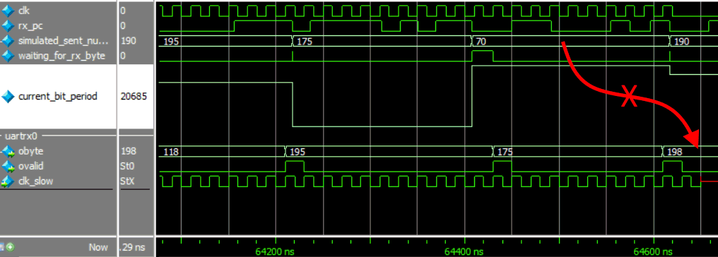 Erroneous byte at 50Mb/s RX UART simulation
So it decoded a received byte 70 as 198. That’s 01000110 and 11000110; it’s got the first bit wrong. Doing this again with a different seed number I found another error during the random bit period test; again it missed the first bit.
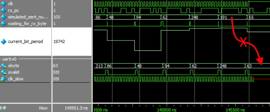 Another erroneous byte at 50Mb/s RX UART simulation
Doing this with a few other seed values in all cases I found the failed byte was sent about 5% slower than it should. Let’s try a max of 4% bit period error and see if that passes all the tests. Yup that seems to have fixed the problem 4% timing error seems to be the upper limit not 5%.
50Mb/s TX UART side
Great so it probably works in real life if the computer could produce 50 Mb per second from the USB to UART converter attached to it, but it can’t. So it looks like the next step is to create the tx component of the 50Mb/s UART. After that it looks like I’ll have to put two UARTs into the FPGA on the development board and another UART on another FPGA and connect those two FPGAs together; argh.
Things that encode or modulate are typically easier to design than decoders and demodulators. Here is a tx UART I designed…
module uarttx
(
	input clk,//baud rate
	input [7:0] txbyte,
	input txload,
	output reg txd,//signal out
	output reg txholding_reg_full
);
reg [7:0] holding_reg=~0;
reg [7:0] shift_reg=~0;
initial txholding_reg_full=0;
reg shift_reg_empty=1;
reg [3:0] shift_reg_ptr=8;
initial txd=1;
reg txload_last=0;
always @(posedge clk)
begin
	//send either shift reg or idle
	if(shift_reg_ptr<=7)
	begin
		txd<=shift_reg[shift_reg_ptr];
		shift_reg_ptr<=shift_reg_ptr+1;
	end
	else
	begin
		shift_reg_empty<=1;
		txd<=1;
	end
	//if +ve edge of load and hold reg empty then either start sending it or move it to the holding reg
	if((txload&&(!txload_last))&&(!txholding_reg_full))
	begin
		if(shift_reg_empty)
		begin
			shift_reg<=txbyte;
			shift_reg_ptr<=0;
			txd<=0;
			shift_reg_empty<=0;
		end
		else
		begin
			holding_reg<=txbyte;
			txholding_reg_full<=1;
		end
	end
	//else if the shift reg has gone empty then start sending the next holding one if available
	else if(shift_reg_empty&&txholding_reg_full)
	begin
		shift_reg<=holding_reg;
		txholding_reg_full<=0;
		shift_reg_ptr<=0;
		txd<=0;
		shift_reg_empty<=0;
	end
	//for keeping track of +ve edge of txload line
	txload_last<=txload;
end
endmodule
That looks reasonably compact in Verilog but in the schematic it’s rather unwieldy and is not particularly pipelined. However, that’s not really a problem as at 50 Mb/s it’s running eight times slower than the rx UART so we can use combinatorial logic that’s eight times as long as we did for the rx side. Now test out by sending two bytes one after another…
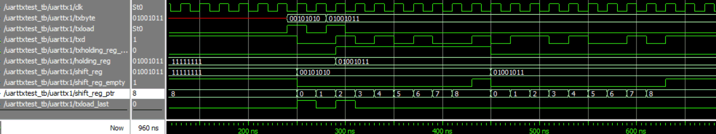 50Mb/s TX UART simulation: sending to bytes
So in this test everything seemed to go correctly, the TXD line outputted the correct data. The txholding_reg_full and shift_reg_empty lines seemed also behave as desired. I then manually changed the distance between loading two bytes and every time it produced the correct TXD output. So now let’s add it to the rx side of the UART.
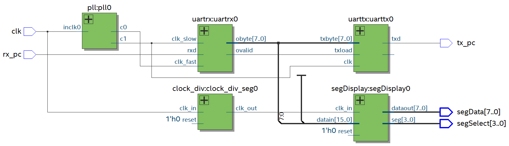 Slow PC UART loopback
So this will loopback the buttons pushed on the computer as well as displaying them on the LED segment display.
It doesn’t check if the transmitter UART is full but instead blindly loads any byte it receives. This raises the obvious fault with the setup which is if the PC is sending data slightly faster than the transmitter UART an overflow will happen and bytes will be lost through the loopback if a long enough continuous stream of bytes from the PC is received. If the PC is sending data slightly slower than the transmitter UART the issue won’t be noticed as no bytes will be dropped. Putting this design on the FPGA and sending large blocks of continuous bytes I noticed that after about 569 bytes I would lose a byte. Increasing the baud rate on the FPGA to 117100b/s even after sending 94,600 bytes continuously through the loopback not one of them got lost. So that strongly suggests that the PC is sending data faster than the FPGA thinks it should do. Anyway I’m not going to bother with this at the moment and am going to call that the UART works.
Clock domain crossing a pesky elephant in the room
For this slow PC loopback the output of the rx UART and the input of the rx UART were running at 115200Hz; this is slow. Say I wanted the output of the rx UART to be synchronous with the main 50MHz input clock to the board. Well for the current rx UART, whilst the two clocks with respect to each other are synchronous, 115200 and 50000000 have a ratio of 36/15625 which is not nice so timing analysis is not going to be able to easily meet the timing requirements. In fact I tried it and I couldn’t get timing closure and when running the design in real life I would sometimes get erroneous bytes. So that means we have to move data from one clock domain to the other. From what I read this is a large subject. Like the other things I’ve done so far I wanted to design my own crossing without blindly using someone else’s black box so I could learn a little. Unlike the single bit synchronizer that I mentioned previously, I can’t use that running many of those in parallel as the data might not necessarily appear at the same time at the destination through all the single bit synchronizers. So my idea was to use one of the single bit synchronizers for a control message to notify the destination to read a register. The source would promise that it would load the register and notify the destination through the synchronizer at the same time whilst not modifying the register until a timeout happened. The notification message will take time to get through the synchronizer and thus the output of the register will settle before the destination reads it. The notification message is encoded by transition. The following schematic shows this design with the nets colored red being ones involved crossing the two clock domains…
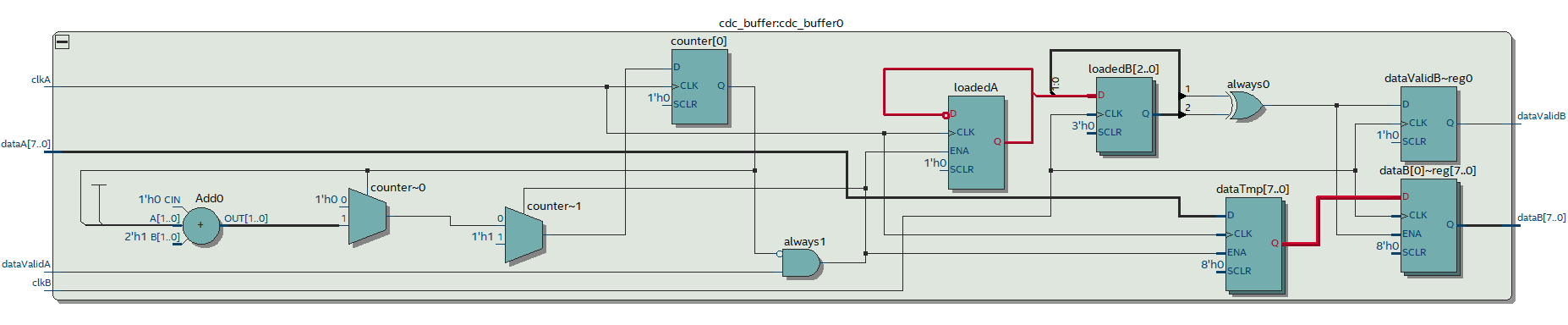 CDC buffer for connecting two clock domains
As Verilog after adding a OK to send line it looks like the following…
module cdc_buffer
#(
	parameter N=8,
	parameter SYNC_LEN=2,
	parameter FREQUENCYA=31.25,
	parameter FREQUENCYB=50.00
)
(
	input clkA,
	input [N-1:0] dataA,
	input dataValidA,
	output AOKToSend,
	input clkB,
	output reg [N-1:0] dataB,
	output reg dataValidB
);

initial dataValidB=0;
reg loadedA=0;
reg [N-1:0] dataTmp;
reg [SYNC_LEN:0] loadedB=0;
always @(posedge clkB)
begin
	loadedB<={loadedB[SYNC_LEN-1:0],loadedA};
	if((loadedB[SYNC_LEN-1])^(loadedB[SYNC_LEN]))
	begin
		dataB<=dataTmp;
		dataValidB<=1;
	end
	else dataValidB<=0;
end

localparam real COUNTER_MAX_REAL=(SYNC_LEN+1)*FREQUENCYA/FREQUENCYB+0.5;
localparam integer COUNTER_MAX=COUNTER_MAX_REAL;
initial $display("COUNTER_MAX_REAL=%f COUNTER_MAX=%d $clog2(COUNTER_MAX)=%d",COUNTER_MAX_REAL,COUNTER_MAX,$clog2(COUNTER_MAX));
reg [$clog2(COUNTER_MAX):0] counter=0;
always @(posedge clkA)
begin
	if(|counter)counter<=counter-1'b1;
	if((counter==0)&&(dataValidA))
	begin
		counter<=COUNTER_MAX;
		loadedA<=!loadedA;
		dataTmp<=dataA;
	end
end
assign AOKToSend=(counter==0);

endmodule
Running a RTL simulation inputting one byte I got the following…
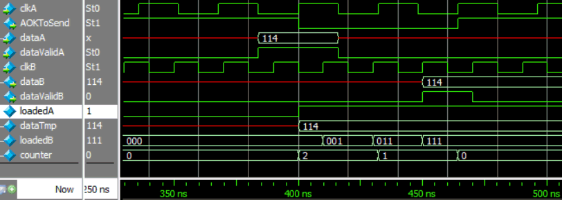 CDC buffer RTL simulation result
You can see that AOKToSend happened after the destination received the sent byte hence no hold violation. That’s very important as the sender promises not to send the next byte until the receiver receives it. Also notice that 3 clkB have happened after the sender has loaded byte into the temp register, this gives plenty of time for the temp register to settle before the receiver reads it so no setup violation. So I think I’ve got the timing values correct but I need to test more. Really I should be doing some gate level simulation but that’s a hassle so I think I’ll just do some more RTL simulations and see if I can find any mistakes.
 CDC buffer RTL simulation result still good
The closest I managed to get it to failing was sending one byte then send the next byte before the AOKToSend line would go high and have the clocks very similar to one another. This produced three cycles before the data was latched and about one cycle of hold time. So it looks like the data will be present on dataTmp at least one clock A cycle before it gets latched into dataB and also at least one clock A cycle after it gets latched into dataB; that’s heaps of time. Now we have to tell the compiler to not be so strict with the wires that cross between the two domains (these were the nets colored red in the schematic) else timing analysis will still fail. For the slow 115200 pc loopback the period of the A side is 8681ns, as that so huge we could create false paths for the nets in the SDC file as follows assuming we have instantiated the CDC buffer as cdc_buffer0…
set_false_path -from {cdc_buffer:cdc_buffer0|dataTmp[*]} -to {cdc_buffer:cdc_buffer0|dataB[*]}
set_false_path -from {cdc_buffer:cdc_buffer0|loadedA} -to {cdc_buffer:cdc_buffer0|loadedB[0]}
However, this just tells the compiler to forget about even attempting to constrain the timing between these wires. We do have a constraint and that is that dataTemp has less than 8681ns to get to dataB (minus some setup time). So let’s be very generous and say our constraint is that the maximum delay the compiler is allowed to create is 4000ns. In the timing analysis tool there is a constraints → set maximum delay option; so let’s give that a go…
set_max_delay -from {cdc_buffer:cdc_buffer0|dataTmp[*]} -to {cdc_buffer:cdc_buffer0|dataB[*]} 4000
set_max_delay -from {cdc_buffer:cdc_buffer0|loadedA} -to {cdc_buffer:cdc_buffer0|loadedB[0]} 4000
Firstly I’ll put the following together where I will use the old slow tx UART. This one uses the standard 50 MHz clock input so it’s data needs to be synchronized with that and hence the need for the CDC buffer…
 Loopback with CDC buffer
Compiling this without the set_max_delay or set_false_path directive mentioned above I got the following in worst paths (red are failing)…
 Compiling without set_max_delay or set_false_path
Compiling with the set_max_delay mentioned above I got the following in worst paths (all pass)…
 Compiling with set_max_delay
Loading in into the FPGA and testing it out in real life also seem to work fine. I increased the tx UART by 100b/s and after transmitting quarter of a million bytes I didn’t lose one.
You can make the previous fast tx UART into a slow tx UART using a bit strobe, for example…
module uarttx_slow
#(
	parameter ClkFrequency = 50000000, // 50MHz
	parameter Baud = 115200,
	parameter Max_error=0.01 //1%
)
(
	input clk,//baud rate
	input [7:0] txbyte,
	input txload,
	output reg txd,//signal out
	output reg txholding_reg_full
);

reg [7:0] holding_reg=~0;
reg [7:0] shift_reg=~0;
initial txholding_reg_full=0;
reg shift_reg_empty=1;
reg [3:0] shift_reg_ptr=8;
initial txd=1;
reg txload_last=0;

reg loadit=0;
reg [7:0] whattoload;

//bit strobe for enable
wire txstrobe;
baud_tick
#(
	.ClkFrequency(ClkFrequency),
	.Baud(Baud),
	.Max_error(Max_error)
)
uarttx0_baud_tick
(
	.clk_in(clk),
	.tick_out(txstrobe)
);

always @(posedge clk)
begin

	txload_last<=txload;
	if((txload&&(!txload_last))&&(!loadit))
	begin
		whattoload<=txbyte;
		loadit<=1;
	end

	if(txstrobe)
	begin

		//send either shift reg or idle
		if(shift_reg_ptr<=7)
		begin
			txd<=shift_reg[shift_reg_ptr];
			shift_reg_ptr<=shift_reg_ptr+1;
		end
		else
		begin
			shift_reg_empty<=1;
			txd<=1;
		end

		//if +ve edge of load and hold reg empty then either start sending it or move it to the holding reg
		if(loadit&&(!txholding_reg_full))
		begin
			loadit<=0;
			if(shift_reg_empty)
			begin
				shift_reg<=whattoload;
				shift_reg_ptr<=0;
				txd<=0;
				shift_reg_empty<=0;
			end
			else
			begin
				holding_reg<=whattoload;
				txholding_reg_full<=1;
			end

		end
		//else if the shift reg has gone empty then start sending the next holding one if available
		else if(shift_reg_empty&&txholding_reg_full)
		begin
			shift_reg<=holding_reg;
			txholding_reg_full<=0;
			shift_reg_ptr<=0;
			txd<=0;
			shift_reg_empty<=0;
		end

	end

end

endmodule

module baud_tick
#(
parameter ClkFrequency = 50000000, // 50MHz
parameter Baud = 115200,
parameter Max_error=0.01 //1%
)
(
input clk_in, //clock in
output tick_out //a high for one clock cycle when time. The period may vary to keep the average period equal to Baud
);
//I dont trust any number of size 31:0 here (some intermediates can be bigger and then do fail) so make them bigger, I'm not sure how to cast like in C. Not sure if [127:0]*[2:0] or [127:0]+[2:0] produces what is expected or not.
localparam [127:0] Baud_BIG=Baud;
localparam [127:0] ClkFrequency_BIG=ClkFrequency;

//calc acc width for error
//this sucks. i can't make a function that takes real values and works out the min val by stepping through BaudGeneratorAccWidth
//to find the min value. all I can do is do the upperbound. is system verilog any better????
//if i create a function it says real unsupported
localparam real ClkFrequency_real=ClkFrequency;
localparam real Baud_real=Baud;
localparam real tmp_val_real=ClkFrequency_real/(2.0*Baud_real*Max_error);
localparam integer tmp_val_int=tmp_val_real;
localparam BaudGeneratorAccWidth=$clog2(tmp_val_int);

initial
begin
	$display("BaudGeneratorAccWidth: %d",BaudGeneratorAccWidth);
end

localparam BaudGeneratorInc = (((Baud_BIG)<<BaudGeneratorAccWidth)+(ClkFrequency_BIG>>1))/(ClkFrequency_BIG);
reg [BaudGeneratorAccWidth:0] BaudGeneratorAcc=0;
always @(posedge clk_in)
begin
	BaudGeneratorAcc <= BaudGeneratorAcc[BaudGeneratorAccWidth-1:0] + BaudGeneratorInc[BaudGeneratorAccWidth:0];
end
assign tick_out = BaudGeneratorAcc[BaudGeneratorAccWidth];
endmodule
`endif
You could tidy it up but you get the idea, it’s being clock at 50 MHz but the flip-flops are being enabled only on some of those positive going edges of that 50 MHz clock.
I’m not sure about this CDC buffer. It seems to be a variation of something called a mux synchronizer. I purposely didn’t put an acknowledgment in as I felt that could cause a lock up if something went wrong. However the one I have is not without its issues either, it has a counter in it which can get rather large. With the current location of the CDC buffer, data is only occasionally going in and really the timeout is not really necessary as data going into the CDC buffer is limited by the baud rate. So let’s simplify it a bit by removing the timer…
module cdc_buffer_simple
#(
	parameter N=8,
	parameter SYNC_LEN=2
)
(
	input clkA,
	input [N-1:0] dataA,
	input dataValidA,
	input clkB,
	output reg [N-1:0] dataB,
	output reg dataValidB
);
initial dataValidB=0;
reg loadedA=0;
reg [N-1:0] dataTmp;
reg [SYNC_LEN:0] loadedB=0;
always @(posedge clkB)
begin
	loadedB<={loadedB[SYNC_LEN-1:0],loadedA};
	if((loadedB[SYNC_LEN-1])^(loadedB[SYNC_LEN]))
	begin
		dataB<=dataTmp;
		dataValidB<=1;
	end
	else dataValidB<=0;
end
always @(posedge clkA)
begin
	if(dataValidA)
	begin
		loadedA<=!loadedA;
		dataTmp<=dataA;
	end
end
endmodule
We could use the fast rx and tx UARTs and connect them together using two of these CDC buffers such that between these two buffers everything will be synchronized to the 50 MHz master clock…
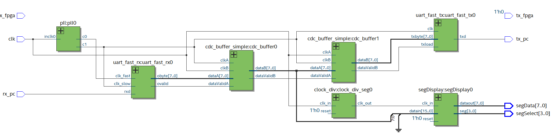 Two CDC buffers and two fast UARTs running slowly
So everything is on the same bus synchronized of the 50 MHz master clock, the segment display driver still with its dodgy connection.
Problems
I’ve had lots of problems so far but I am now experiencing some weird ones that I have yet to fully understand. I have noticed that slight changes made to the SDC constraints file, compiler settings, or the design will cause the design to either fail or work in real life. For example adding some input registers to segDisplay will cause the loopback to fail even though it shouldn’t have anything to do with the path from rx_pc to tx_pc. For a failing real life test changing the rx_pc rxd path from a false path to one with some random maximum and minimum delays causes the design to work again. Some slight changes will even cause LEDs to light even though they aren’t assigned in the pin planner to do anything. So yes some very strange problems indeed.
The following image the digit that is showing 9 is actually not assigned any pin in the pin planner. The loopback worked fine just this strange digit that would be the overlap of all the other three digits to the left of it. To get it to do this I selected performance aggressive from the compiler settings and a false path for the rx_pc rxd path. Selecting normal performance mode didn’t produce this extra LED to light up. P136 of the FPGA is supposed to drive this LED segment and by default all unassigned pins should be tri-state high.
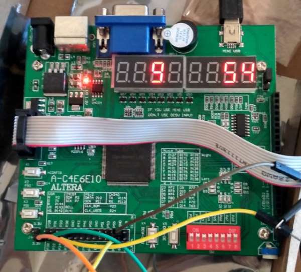 One segment erroneously illuminated
Looking at P136 with the oscilloscope the pin was indeed being driven low and I measured 0 V on it. Ahh, I think I see this one now. Although my QSF file has the following pin placement…
set_location_assignment PIN_23 -to clk
set_location_assignment PIN_114 -to rx_pc
set_location_assignment PIN_113 -to tx_pc
set_location_assignment PIN_115 -to segData[7]
set_location_assignment PIN_119 -to segData[6]
set_location_assignment PIN_120 -to segData[5]
set_location_assignment PIN_121 -to segData[4]
set_location_assignment PIN_124 -to segData[3]
set_location_assignment PIN_125 -to segData[2]
set_location_assignment PIN_126 -to segData[1]
set_location_assignment PIN_127 -to segData[0]
set_location_assignment PIN_133 -to segSelect[3]
set_location_assignment PIN_132 -to segSelect[2]
set_location_assignment PIN_129 -to segSelect[1]
set_location_assignment PIN_128 -to segSelect[0]
In my schematic I had defined the pin called tx_fpga that I didn’t connect anything. I had assumed if I didn’t connect it to anything the compiler wouldn’t connect it to anything. However looking at the pin planner tool I see the following…
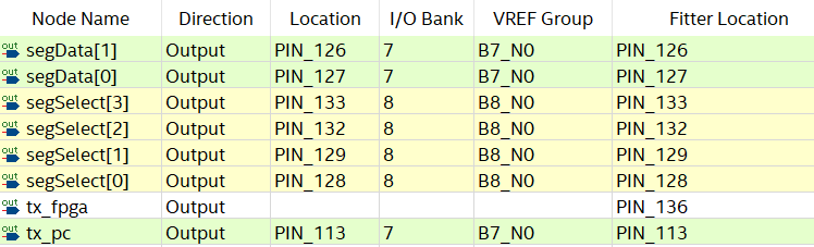 Be careful to define the location of all pins
So what looks like has happened is the fitter sometimes connects pins that have not been explicitly defined to physical FPGA pins; but not always. It’s crazy the fitter isn’t consistent about connecting the pin or not. That’s weird and definitely a gotcha. Lesson learnt; always explicitly define locations of all output pins even if they aren’t used else the fitter might have a field day.
One problem fixed one to go. This one might be a lot harder and seems any slight change in the SDC file, compiler settings or design will make it appear or disappear. The loopback fails to work correctly and sometimes sending a byte will produce the wrong byte being displayed both by the PC and on the segment display. What is always consistent is that what is displayed on the segment display is always the same as displayed on the PC. This suggests it’s a problem with rx UART or the CDC buffer. I couldn’t get the issue to appear if I directly connected the segment display to the output of the rx UART or didn’t connect the segment display at all; it was a tricky to make appear. When it failed in real life, gate level simulations still all worked no matter what I threw at them.
One thing I noticed is the compiler didn’t complain about the connection from the CDC buffer to the segment display driver even though that’s clearly a clock domain crossing putting the following in to the SDC file made it work in real life…
set_false_path -from {cdc_buffer_simple:cdc_buffer0|*} -to {segDisplay:segDisplay0|*}
But I’m not sure is the reason for this problem as changing pretty much anything causes the problem to seemingly vanish and I couldn’t get the problem to occur even with gate level simulations. So for now I’ll assume it’s some sort of constraint issue (maybe not constraining the asynchronous input enough?) and move on but also aware that I may have to revisit it later.
Here’s another strange issue. In the RTL viewer sometimes if you zoom into a module then zoom out of the module the connections change. This can be seen in the following two figures were I zoomed into the bin2bcd module then out again and you can see it’s connected a whole lot of the output wires to ground. This looks very much like a Quartus bug.
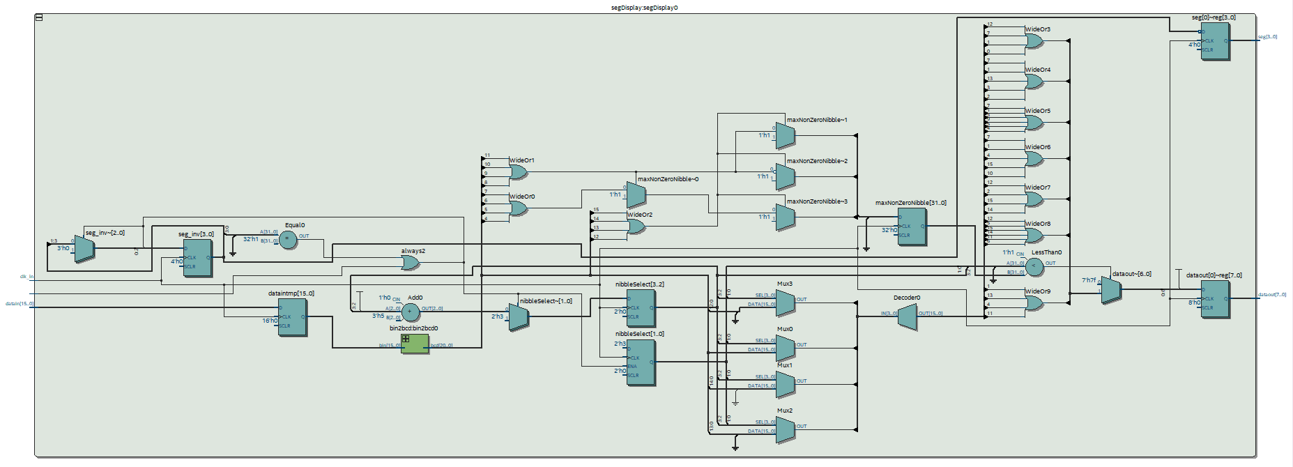 Before zooming in to a submodule
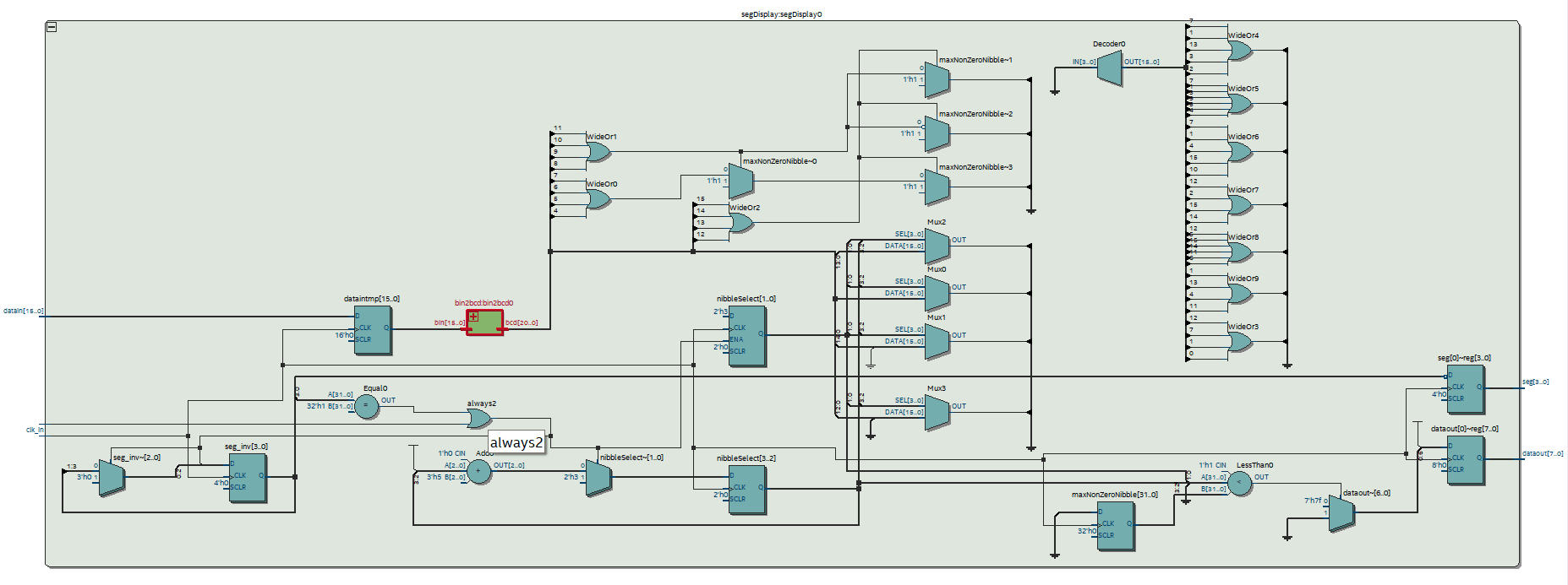 Upon exit of the submodule the schematic is now erroneous
Tidying up the segment display driver
The segment display driver is a bit of a mess so let’s get it working a little bit better and so it doesn’t require being run in a different clock domain. Also as we can display up to eight digits let’s create a dual display so four digits can be for data coming from the PC side and the other four can be used for data coming from the 50 Mb/s side.
Here is the dual display…
`ifndef SEGDUALDISPLAY_H
`define SEGDUALDISPLAY_H

`include "segDisplay.sv"
`include "bit_tick.sv"

module segDualDisplay
#(
parameter SEGS = 4, //# of segs to use for each display
parameter DROP_LEADING_ZEROS = 1, // if set to 1 then leading zeros wont be displayed
parameter DIPLAY_AS_DEC = 1, // if 1 then datain will be displayed as dec else will be displayed as hex
parameter ClkFrequency = 50000000,
parameter LED_UPDATE_RATE = 90,
parameter Max_error = 0.25 //for 90Hz --> 67.5Hz to 112.5Hz
)
(
	input wire clk,
	input wire [(4*SEGS)-1:0] datain1,
	input wire [(4*SEGS)-1:0] datain2,
	output reg[7:0] dataout,
	output reg[((2*SEGS)-1):0] seg12
);

//bit strobe for led seg advance
wire ledstrobe;
bit_tick
#(
	.ClkFrequency(ClkFrequency),
	.Baud(LED_UPDATE_RATE*SEGS*2),
	.Max_error(Max_error)
)
ledstrobe_bit_tick
(
	.clk_in(clk),
	.tick_out(ledstrobe)
);

wire [7:0] dataout_wire0;
wire [7:0] dataout_wire1;
wire [(SEGS-1):0] seg_wire0;
wire [(SEGS-1):0] seg_wire1;
initial seg12=~0;
reg bankSelect=0;

always @(posedge clk)
begin
	if(ledstrobe)
	begin
		bankSelect<=~bankSelect;
//		seg12<=bankSelect?{seg_wire0,4'b1111}:{4'b1111,seg_wire1};
//		dataout<=bankSelect?dataout_wire0:dataout_wire1;
	end
end

always @(*)
begin
	seg12=bankSelect?{seg_wire0,4'b1111}:{4'b1111,seg_wire1};
	dataout=bankSelect?dataout_wire0:dataout_wire1;
end

segDisplay
#(
.SEGS(SEGS),
.DROP_LEADING_ZEROS(DROP_LEADING_ZEROS),
.DIPLAY_AS_DEC(DIPLAY_AS_DEC)
)
segDisplay0
(
	.clk(clk),
	.seg_update_strobe(bankSelect&ledstrobe),
	.datain(datain1),
	.dataout(dataout_wire0),
	.seg(seg_wire0)
);

segDisplay
#(
.SEGS(SEGS),
.DROP_LEADING_ZEROS(DROP_LEADING_ZEROS),
.DIPLAY_AS_DEC(DIPLAY_AS_DEC)
)
segDisplay1
(
	.clk(clk),
	.seg_update_strobe((~bankSelect)&ledstrobe),
	.datain(datain2),
	.dataout(dataout_wire1),
	.seg(seg_wire1)
);

endmodule

`endif
It creates a strobe for updating the two segment displays using a module called bit_tick. The two segment displays are alternately lit up using a bank select wire. The segment display module looks like the following…
`ifndef SEGDISPLAY_H
`define SEGDISPLAY_H

`include "bin2bcd.sv"

module segDisplay
#(
parameter SEGS = 4, //# of segs to use
parameter DROP_LEADING_ZEROS = 1, // if set to 1 then leading zeros wont be displayed
parameter DIPLAY_AS_DEC = 1 // if 1 then datain will be displayed as dec else will be displayed as hex
)
(
	input wire clk,
	input wire seg_update_strobe,
	input wire [(4*SEGS)-1:0] datain,
	input wire reset,
	output reg[7:0] dataout=0,
	output reg[SEGS-1:0] seg=~0
);

reg [(4*SEGS)-1:0] dataintmp;

always @(posedge clk)
begin
	dataintmp<=datain;
end

reg [SEGS-1:0] seg_inv=(1<<(SEGS-1));//1;

//convert from bin to bcd if needed
wire [(4*SEGS)+((4*SEGS)-4)/3:0] bcd;
wire [(4*SEGS)-1:0] datain_local;
assign datain_local=DIPLAY_AS_DEC?bcd:dataintmp;
bin2bcd
#(.W(4*SEGS))  // input width
bin2bcd0
(
	.bin(dataintmp),  // binary in
	.bcd(bcd) //bcd out
);

//for dataout and seg given datain_local and nibbleSelect
integer maxNonZeroNibble;
integer i;
reg [($clog2(4*SEGS))-1:0] nibbleSelect=((4*SEGS)-1);
wire [3:0] CurrentSegDigit;
assign CurrentSegDigit=(datain_local[nibbleSelect -: 4]);
always @ ( posedge clk )
begin

	if(seg_update_strobe)
	begin

		seg<=~seg_inv;

		//find max nibble that is non zero else say the last nibble is non zero even if it's not so as to display a zero.
		maxNonZeroNibble<=4;
		for(i=1;i<SEGS;i=i+1)
		begin
			if(|datain_local[4*i+3 -: 4])maxNonZeroNibble<=(4*i+3);
		end

		if((!DROP_LEADING_ZEROS)||(nibbleSelect<=maxNonZeroNibble))
		begin
			case ( CurrentSegDigit )
			0: dataout<=8'b11000000;
			1: dataout<=8'b11111001;
			2: dataout<=8'b10100100;
			3: dataout<=8'b10110000;
			4: dataout<=8'b10011001;
			5: dataout<=8'b10010010;
			6: dataout<=8'b10000010;
			7: dataout<=8'b11111000;
			8: dataout<=8'b10000000;
			9: dataout<=8'b10010000;
			10:dataout<=8'b10001000;
			11:dataout<=8'b10000011;
			12:dataout<=8'b11000110;
			13:dataout<=8'b10100001;
			14:dataout<=8'b10000110;
			15:dataout<=8'b10001110;
			default: dataout<=8'b11101111;
			endcase
		end
		else dataout<=8'b11111111;

	end

end

//tring out tasks.

task reset_task();
begin
	seg_inv<=(1<<(SEGS-1));
	nibbleSelect<=((4*SEGS)-1);
end
endtask

task next_nibble_task();
begin
	seg_inv<=(seg_inv>>1);
	nibbleSelect<=(nibbleSelect-4);
end
endtask

//seq for updating nibbleSelect and seg_inv
always @ (  posedge clk )
begin
	if(seg_update_strobe)
	begin
		if((reset)||(seg_inv==1))reset_task();//first seg is MSN
		else next_nibble_task();//shift to the next nibble
	end
end

endmodule

`endif
On any positive edge of the clock it tests to see if the strobe is active this gets rid of the clock crossing the main problem that I had before. Then there’s the binary to BCD converter that I copied from Wikipedia…
// parametric Verilog implementation of the double dabble binary to BCD converter
// for the complete project, see
// https://github.com/AmeerAbdelhadi/Binary-to-BCD-Converter

`ifndef BIN2BCD_H
`define BIN2BCD_H

module bin2bcd
 #( parameter                W = 18)  // input width
  ( input      [W-1      :0] bin   ,  // binary
    output reg [W+(W-4)/3:0] bcd   ); // bcd {...,thousands,hundreds,tens,ones}

  integer i,j;

  always @(bin) begin
    for(i = 0; i <= W+(W-4)/3; i = i+1) bcd[i] = 0;     // initialize with zeros
    bcd[W-1:0] = bin;                                   // initialize with input vector
    for(i = 0; i <= W-4; i = i+1)                       // iterate on structure depth
      for(j = 0; j <= i/3; j = j+1)                     // iterate on structure width
        if (bcd[W-i+4*j -: 4] > 4)                      // if > 4
          bcd[W-i+4*j -: 4] = bcd[W-i+4*j -: 4] + 4'd3; // add 3
  end

endmodule

`endif
And finally the bit_tick module used to create the strobe with more angry comments than design…
`ifndef BIT_TICK_H
`define BIT_TICK_H
module bit_tick
#(
parameter ClkFrequency = 50000000, // 50MHz
parameter Baud = 115200,
parameter Max_error=0.01 //1%
)
(
input clk_in, //clock in
output tick_out //a high for one clock cycle when time. The period may vary to keep the average period equal to Baud
);
//I dont trust any number of size 31:0 here (some intermediates can be bigger and then do fail) so make them bigger, I'm not sure how to cast like in C. Not sure if [127:0]*[2:0] or [127:0]+[2:0] produces what is expected or not.
localparam [127:0] Baud_BIG=Baud;
localparam [127:0] ClkFrequency_BIG=ClkFrequency;

//calc acc width for error
//this sucks. i can't make a function that takes real values and works out the min val by stepping through BaudGeneratorAccWidth
//to find the min value. all I can do is do the upperbound.
//if i create a function it says real unsupported. I dont want to Synthesize it I just want to use it to preprocess.
//come on this is sooooooo stupid!!!!!!!!!!!!!!!!!!!!!!!!!!!!!!!!!!!!!!!!!!!!!!!!!!!!!!!!
//i cant even use $display with some calc in it. come on who is writing the specs???
localparam real ClkFrequency_real=ClkFrequency;
localparam real Baud_real=Baud;
localparam real tmp_val_real=ClkFrequency_real/(2.0*Baud_real*Max_error);
localparam integer tmp_val_int=tmp_val_real;
localparam BaudGeneratorAccWidth=$clog2(tmp_val_int);

initial
begin
	$display("bit_tick Baud=%d BaudGeneratorAccWidth=%d BaudGeneratorInc=%d {this stupid thing cant even calulate exact step (%f*2^%f)/%f} or exact hz %f*%f/(2^%f)",Baud,BaudGeneratorAccWidth,BaudGeneratorInc,Baud,BaudGeneratorAccWidth,ClkFrequency,BaudGeneratorInc,ClkFrequency,BaudGeneratorAccWidth);
end

localparam BaudGeneratorInc = (((Baud_BIG)<<BaudGeneratorAccWidth)+(ClkFrequency_BIG>>1))/(ClkFrequency_BIG);
reg [BaudGeneratorAccWidth:0] BaudGeneratorAcc=0;
always @(posedge clk_in)
begin
	BaudGeneratorAcc <= BaudGeneratorAcc[BaudGeneratorAccWidth-1:0] + BaudGeneratorInc[BaudGeneratorAccWidth:0];
end
assign tick_out = BaudGeneratorAcc[BaudGeneratorAccWidth];
endmodule

`endif
Slow UART tidy up
I did a quick tidy up of the slow UART but it’s basically the same thing it was when I originally wrote it…
//8N1 uart
`include "baud_tick.sv"

module uart_slow_rx
#(
parameter ClkFrequency = 50000000, // 50MHz
parameter Baud = 115200,
parameter Max_error=0.01
)
(
	input clk,
	input rxd,
	output reg data_out_valid,
	output reg [7:0] data_out,
	output BitTick
);

initial data_out_valid=0;

localparam START_BIT_PATTERN = 2'b10;

reg RxD_sync_last;//=0;
reg [7:0] data_shift;//=0;
integer frame_cnt=10;

//make the RxD line sync with the clk. this stops metastable things
reg RxD_sync;//=1;
reg rxd_temp;//=1;
always @(posedge clk)
begin
	rxd_temp<=rxd;
	RxD_sync<=rxd_temp;
end

//when stop bit is sampled start resetting
wire baud_reset=(frame_cnt>=10)?1'b1:1'b0;

//baud tick
baud_tick #(.ClkFrequency(ClkFrequency),.Baud(Baud),.Max_error(Max_error),.MidResetDelayCompensation(2)) baud_tick_rx(clk,BitTick,baud_reset,1'b0);

//when shift register is full load into output register
always @(posedge clk)
begin
	if((frame_cnt==9)&&(BitTick))//done on stop bit
	begin
		data_out_valid<=1;
		data_out<=data_shift;
	end
	else data_out_valid<=0;
end

//when resetting wait for high low transition
wire start_sense=(({RxD_sync_last,RxD_sync}==START_BIT_PATTERN)&&(baud_reset))?1'b1:1'b0;
always @(posedge clk)
begin
	RxD_sync_last<=RxD_sync;
end

//deal with frame counter and shifting data into register as it comes along
always @(posedge clk)
begin
	if(baud_reset)
	begin
		if(start_sense)frame_cnt<=0;
	end
	else if(BitTick)
	begin
		frame_cnt<=frame_cnt+1;
		data_shift<={RxD_sync,data_shift[7:1]};
	end
end

endmodule
It uses a module called baud_tick which is almost the same as bit_tick but it has some reset lines to allow the UART receiver to reset for half the period It would normally reset for so as to allow sampling between symbol transitions. baud_tick is here…
`ifndef BAUD_TICK_H
`define BAUD_TICK_H
module baud_tick
#(
parameter ClkFrequency = 50000000, // 50MHz
parameter Baud = 115200,
parameter MidResetDelayCompensation = 3,
parameter ResetDelayCompensation = 1,
parameter Max_error=0.01 //1%
)
(
input clk_in, //clock in
output tick_out, //a high for one clock cycle when time. The period may vary to keep the average period equal to Baud
input mid_reset, //mid_reset holds start period at about 1/2 T (T=(1/Baud)) so that when releasing the first tick_out happens in 1/2 T seconds which is handy for the rx uart
input reset //zero reset
);
//I dont trust any number of size 31:0 here (some intermediates can be bigger and then do fail) so make them bigger, I'm not sure how to cast like in C. Not sure if [127:0]*[2:0] or [127:0]+[2:0] produces what is expected or not.
localparam [127:0] Baud_BIG=Baud;
localparam [127:0] ClkFrequency_BIG=ClkFrequency;

//calc acc width for error
//this sucks. i can't make a function that takes real values and works out the min val by stepping through BaudGeneratorAccWidth
//to find the min value. all I can do is do the upperbound. is system verilog any better????
//if i create a function it says real unsupported
localparam real ClkFrequency_real=ClkFrequency;
localparam real Baud_real=Baud;
localparam real tmp_val_real=ClkFrequency_real/(2.0*Baud_real*Max_error);
localparam integer tmp_val_int=tmp_val_real;
localparam BaudGeneratorAccWidth=$clog2(tmp_val_int);

initial
begin
	$display("BaudGeneratorAccWidth: %d",BaudGeneratorAccWidth);
end

localparam BaudGeneratorInc = (((Baud_BIG)<<BaudGeneratorAccWidth)+(ClkFrequency_BIG>>1))/(ClkFrequency_BIG);
localparam BaudGeneratorMidResetValue=((128'd1)<<(BaudGeneratorAccWidth-1))+MidResetDelayCompensation*BaudGeneratorInc[BaudGeneratorAccWidth:0];//times by 3 due to various delays with the uart rx
localparam BaudGeneratorResetValue=ResetDelayCompensation*BaudGeneratorInc[BaudGeneratorAccWidth:0];
reg [BaudGeneratorAccWidth:0] BaudGeneratorAcc=0;
always @(posedge clk_in)
begin
	if(reset) BaudGeneratorAcc<=BaudGeneratorResetValue;
	 else if(mid_reset)BaudGeneratorAcc<=BaudGeneratorMidResetValue;
	  else BaudGeneratorAcc <= BaudGeneratorAcc[BaudGeneratorAccWidth-1:0] + BaudGeneratorInc[BaudGeneratorAccWidth:0];
end
assign tick_out = BaudGeneratorAcc[BaudGeneratorAccWidth];
endmodule
`endif
You might’ve also noticed that I have changed everything to systemVerilog files (file extension .sv). As Verilog is a subset of SystemVerilog there doesn't seem to be any reason why I shouldn't use it even though I don’t know much about system Verilog.
Putting it all together on the first FPGA board
You’ve already seen the slow transmitter UART and the fast UART so here’s the top level design that connects everything together…
module uartslowfasttest
#(
	parameter ClkFrequency = 50000000,//clk input
	parameter SEGS=8,//4 segs for pc rx uart and 4 segs for fpga rx uart
	parameter LED_UPDATE_RATE=90, //90Hz
	parameter LED_UPDATE_RATE_MAX_ERROR=0.25,//for 90Hz --> 67.5Hz to 112.5Hz (actually produces 95Hz with current code)
	parameter PC_BAUD_RATE=(115200+100),//100Hz faster so loopback doesn't overflow
	parameter PC_BAUD_RATE_MAX_ERROR=0.01, //1% max baud rate error allowed for pc uart
	parameter FPGA_BAUD_RATE=50000000 //bit rate fast fpga uart
)
(
	input clk,//50MHz

	//for pc
	input rx_pc,//signal from pc
	output tx_pc,//signal to pc

	//for other fpga board
	input rx_fpga,//signal from other fpga
	output tx_fpga,//signal to other fpga

	//for leds
	output [7:0] segData,//LED seg data
	output [SEGS-1:0] segSelect//LED seg select

);

//pll for fast uart
wire clk_slow;//baud rate
wire clk_fast;//8*baud rate
pll pll0
(
	clk,		//50MHz int
	clk_fast,//400MHz out
	clk_slow	//50MHz out
);

//-----------------
//---the 4 uarts---
//-----------------

//slow pc rx uart
wire [7:0] rx_pc_byte;
wire rx_pc_byte_valid;
uart_slow_rx
#(
	.ClkFrequency(ClkFrequency),
	.Baud(PC_BAUD_RATE),
	.Max_error(PC_BAUD_RATE_MAX_ERROR)
)
uart_slow_rx0
(
	.clk(clk_slow),
	.rxd(rx_pc),//signal in
	.data_out_valid(rx_pc_byte_valid),
	.data_out(rx_pc_byte)
);

//fast fpga tx uart
uart_fast_tx uart_fast_tx0
(
	.clk(clk_slow),
	.txbyte(rx_pc_byte),
	.txload(rx_pc_byte_valid),
	.txd(tx_fpga)//signal out
);

//fast fpga rx uart
wire [7:0] rx_fpga_byte;//valid when ovalid is high but will not change till ovalid strobes again
wire rx_fpga_byte_valid;//high for 1 bit to mark a valid obyte
uart_fast_rx uart_fast_rx0
(
	.clk_slow(clk_slow),//baud rate
	.clk_fast(clk_fast),//8*baud rate
	.rxd(rx_fpga),//signal in
	.obyte(rx_fpga_byte),//valid when ovalid is high but will not change till ovalid strobes again
	.ovalid(rx_fpga_byte_valid)//high for 1 bit to mark a valid obyte
);

//slow pc tx uart
uart_slow_tx
#(
	.ClkFrequency(ClkFrequency),
	.Baud(PC_BAUD_RATE),
	.Max_error(PC_BAUD_RATE_MAX_ERROR)
)
uart_slow_tx0
(
	.clk(clk_slow),
	.txbyte(rx_fpga_byte),
	.txload(rx_fpga_byte_valid),
	.txd(tx_pc)//signal out
);

//-----------------
//---for display---
//-----------------

//0 to 7 bits are used but 8 to 15 are tied to ground
wire [15:0] dataSegWiresFromPc;
wire [15:0] dataSegWiresFromFPGA;
assign dataSegWiresFromPc=rx_pc_byte;
assign dataSegWiresFromFPGA=rx_fpga_byte;

segDualDisplay
#(
.SEGS(SEGS/2), //# of segs to use for each display
.DROP_LEADING_ZEROS(1), // if set to 1 then leading zeros wont be displayed
.DIPLAY_AS_DEC(1),// if 1 then datain will be displayed as dec else will be displayed as hex
.ClkFrequency(ClkFrequency),
.LED_UPDATE_RATE(LED_UPDATE_RATE),
.Max_error(LED_UPDATE_RATE_MAX_ERROR)
)
segDisplay0
(
	.clk(clk_slow),
	.datain1(dataSegWiresFromPc),
	.datain2(dataSegWiresFromFPGA),
	.dataout(segData),
	.seg12(segSelect)
);

endmodule
The schematic of this looks like the following…
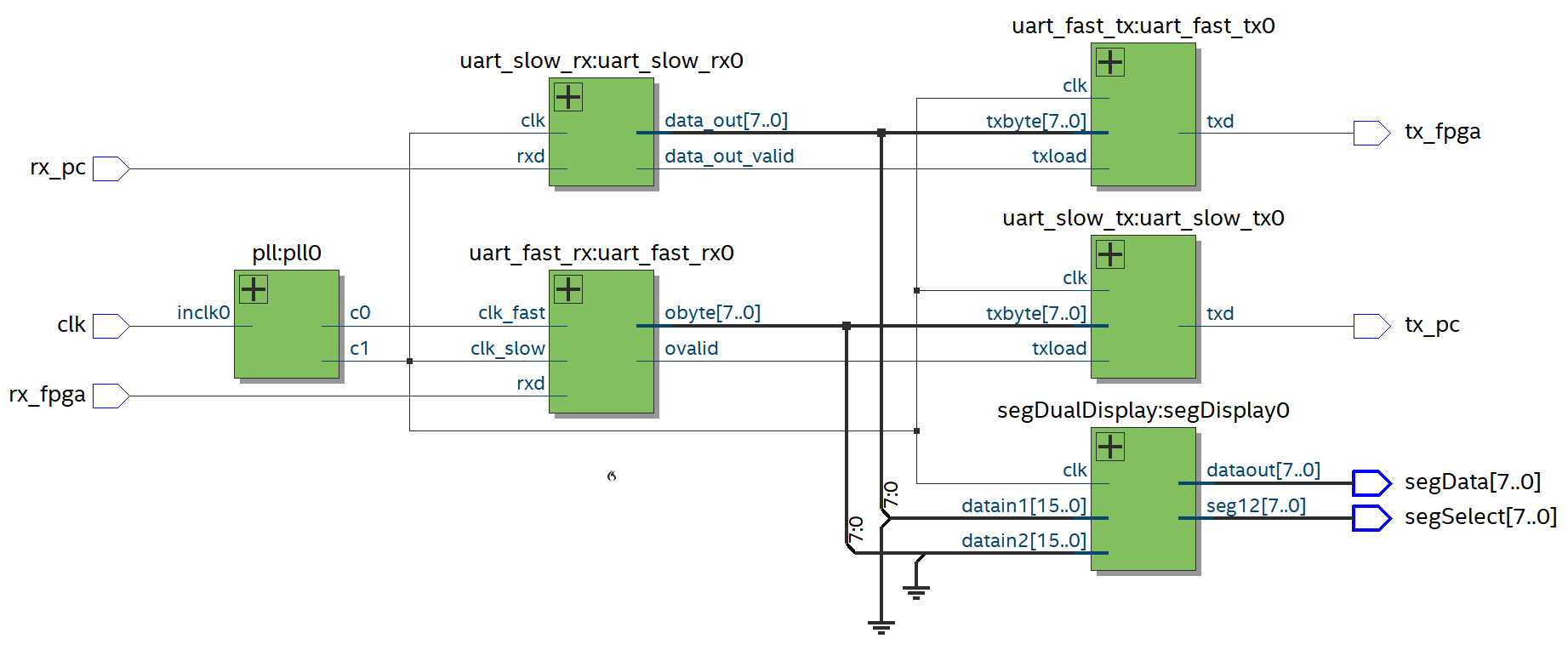 Schematic for 50Mb/s test on 1st FPGA board
You can see the main clock that everything is based off is the 50 MHz clock produced by the PLL. The only thing that uses the 400 MHz clock (clk_fast) is the fast receiving UART.
The false constraints I said as follows…
#**************************************************************
# Set False Path
#**************************************************************

set_false_path -from [get_ports {rx_fpga}] -to {uart_fast_rx:uart_fast_rx0|shift_reg[0]}
set_false_path -from [get_ports {rx_pc}] -to {uart_slow_rx:uart_slow_rx0|rxd_temp}

set_false_path -from {uart_slow_tx:uart_slow_tx0|txd|*} -to [get_ports {tx_pc}]
set_false_path -from {uart_fast_tx:uart_fast_tx0|txd|*} -to [get_ports {tx_fpga}]

set_false_path -from {segDualDisplay:segDisplay0|*} -to [get_ports {segData[*]}]
set_false_path -from {segDualDisplay:segDisplay0|*} -to [get_ports {segSelect[*]}]

Whilst the clock constraints are as follows…

#**************************************************************
# Create Clock
#**************************************************************

create_clock -name {clk} -period 20.000 -waveform { 0.000 10.000 } [get_ports {clk}]

#**************************************************************
# Create Generated Clock
#**************************************************************

create_generated_clock -name {pll0|altpll_component|auto_generated|pll1|clk[0]} -source [get_pins {pll0|altpll_component|auto_generated|pll1|inclk[0]}] -duty_cycle 50/1 -multiply_by 8 -divide_by 1 -master_clock {clk} [get_pins {pll0|altpll_component|auto_generated|pll1|clk[0]}]
create_generated_clock -name {pll0|altpll_component|auto_generated|pll1|clk[1]} -source [get_pins {pll0|altpll_component|auto_generated|pll1|inclk[0]}] -duty_cycle 50/1 -multiply_by 1 -divide_by 1 -master_clock {clk} [get_pins {pll0|altpll_component|auto_generated|pll1|clk[1]}]
In the QSF file I made the following pin assignments to the outside world…
set_location_assignment PIN_23 -to clk
set_location_assignment PIN_114 -to rx_pc
set_location_assignment PIN_113 -to tx_pc
set_location_assignment PIN_115 -to segData[7]
set_location_assignment PIN_119 -to segData[6]
set_location_assignment PIN_120 -to segData[5]
set_location_assignment PIN_121 -to segData[4]
set_location_assignment PIN_124 -to segData[3]
set_location_assignment PIN_125 -to segData[2]
set_location_assignment PIN_126 -to segData[1]
set_location_assignment PIN_127 -to segData[0]
set_location_assignment PIN_138 -to segSelect[7]
set_location_assignment PIN_137 -to segSelect[6]
set_location_assignment PIN_136 -to segSelect[5]
set_location_assignment PIN_135 -to segSelect[4]
set_location_assignment PIN_133 -to segSelect[3]
set_location_assignment PIN_132 -to segSelect[2]
set_location_assignment PIN_129 -to segSelect[1]
set_location_assignment PIN_128 -to segSelect[0]
set_location_assignment PIN_32 -to tx_fpga
set_location_assignment PIN_30 -to rx_fpga
Compiling using the balanced setting I used 434 logic elements (4% of what is available on the FPGA), 255 registers and one of the two PLLs.
Timing analysis passed with an Fmax of 94 MHz for the slow clock and 467 MHz for the fast clock. However it said the fast clock was limited to 402 MHz due to minimum period restrictions. The minimum setup slack for the 1.2 V 85 centigrade slow model was 184 ps and 366 ps for the slow and fast clocks respectively.
I then uploaded the design to the board and tried it both without and with a wire between pin 32 and pin 30 to complete the loopback. Without the wire connected the LEDs on the left-hand side displayed whatever buttons I was pressing on the computer whilst the right LEDs showed no change. With the wire connected both sets of LEDs displayed the same decimal representation of the ASCII character I was pushing on the keyboard.
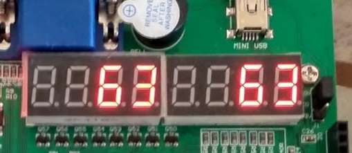 “?” being received by both UARTs
Connecting the tx_fpga pin up to the oscilloscope (a Rigol DS1054) which is only a 50 MHz oscilloscope I took a screen capture of the signal passing down the loopback wire which can be seen in the following figure where I pressed the button "1".
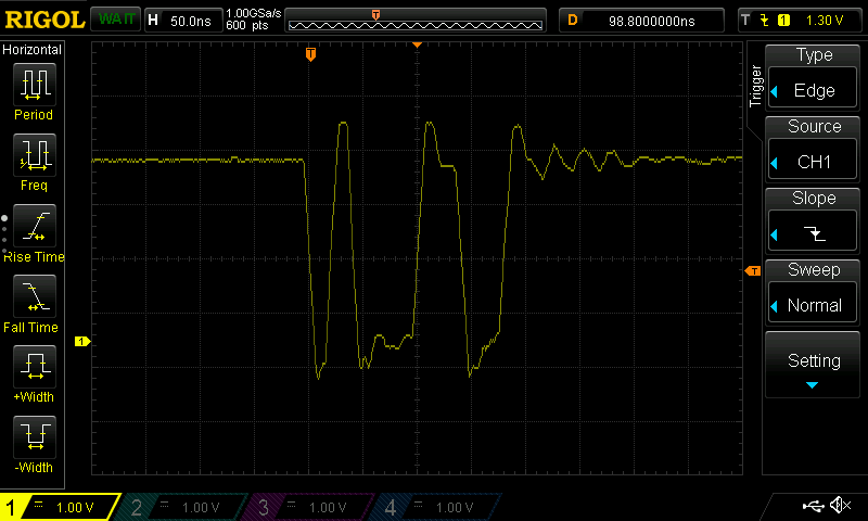 50Mb/s serial in real life: Button "1" pressed
1 in ASCII is 0b00110001. UARTs send everything back to front and prepend a low start bit and a high stop bit. In this screenshot everything is over in about 200 ns. You can see a bit of ringing when the stop bit arrives. Even though it looks not the most elegant display the FPGA had no problems decoding any of the bytes that I sent through it. I sent through thousands of bytes and didn’t detect one error. I found it interesting that the Rigol couldn’t decode serial data at 50 Mb per second. So currently the only thing I have that can decode serial data at this speed is the FPGA board.
Putting it all together on the second FPGA board
I have two FPGA boards the second FPGA board didn’t come populated with any headers and only came with one onboard user LED and two user buttons. However I can solder a couple of wires onto it and put the 50 Mb/s UART into it to do a few more tests.
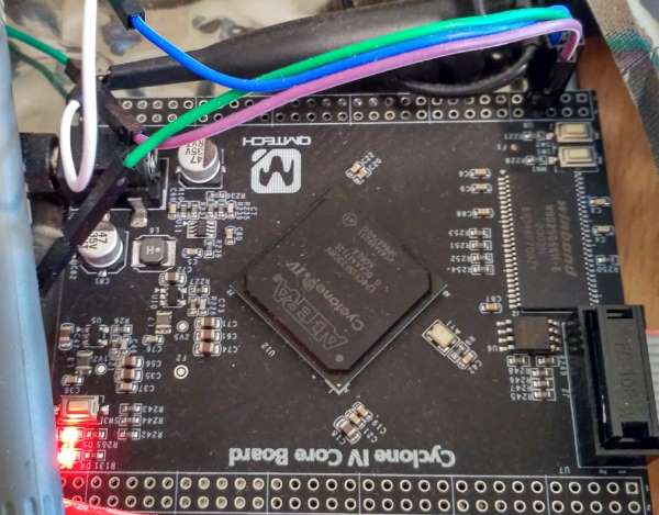 Second FPGA development board
I put the following high-speed UART into the second FPGA board…
module uartfast2ndbrdtest
(
	input clk,//50MHz

	//for other fpga board
	input rx_fpga,//signal from other fpga
	output tx_fpga,//signal to other fpga

	//for led
	output reg led//LED

);

//pll for fast uart
wire clk_slow;//baud rate
wire clk_fast;//8*baud rate
pll pll0
(
	clk,		//50MHz int
	clk_fast,//400MHz out
	clk_slow	//50MHz out
);

//-----------------
//---the 2 uarts---
//-----------------

//fast fpga rx uart
wire [7:0] rx_fpga_byte;//valid when ovalid is high but will not change till ovalid strobes again
wire rx_fpga_byte_valid;//high for 1 bit to mark a valid obyte
uart_fast_rx uart_fast_rx0
(
	.clk_slow(clk_slow),//baud rate
	.clk_fast(clk_fast),//8*baud rate
	.rxd(rx_fpga),//signal in
	.obyte(rx_fpga_byte),//valid when ovalid is high but will not change till ovalid strobes again
	.ovalid(rx_fpga_byte_valid)//high for 1 bit to mark a valid obyte
);

//fast fpga tx uart
uart_fast_tx uart_fast_tx0
(
	.clk(clk_slow),
	.txbyte(rx_fpga_byte),
	.txload(rx_fpga_byte_valid),
	.txd(tx_fpga)//signal out
);

//----------------

initial led=0;
always @(posedge clk_slow) if(rx_fpga_byte_valid)led=~led;

endmodule
Connecting up the oscilloscope I looked at the connections between the two FPGA boards this can be seen in the following figure…
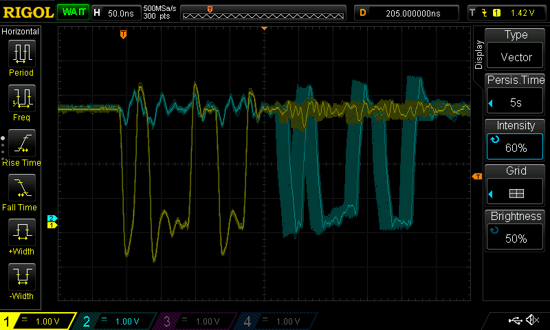 50 Mb/s signal going in (yelllow) and out (blue) of the second FPGA development board
The yellow trace is coming out of the first FPGA board going into the second FPGA board. The second FPGA is decoding the signal reencoding it and then sending it back which can be seen as the blue trace. I had some persistence on so I could see the minimum and maximum delays through the second FPGA board. The delay between the second board receiving the stop bit of the yellow trace and sending the start bit of the blue trace is about 55ns10ns.
I then changed the code on the second FPGA board to the following…
module uartfast2ndbrdtest
(
	input clk,//50MHz

	//for other fpga board
	input rx_fpga,//signal from other fpga
	output tx_fpga,//signal to other fpga

	//for led
	output reg led//LED
);

//pll for fast uart
wire clk_slow;//baud rate
wire clk_fast;//8*baud rate
pll pll0
(
	clk,		//50MHz int
	clk_fast,//400MHz out
	clk_slow	//50MHz out
);

//-----------------
//---the 2 uarts---
//-----------------

//fast fpga rx uart
wire [7:0] rx_fpga_byte;//valid when ovalid is high but will not change till ovalid strobes again
wire rx_fpga_byte_valid;//high for 1 bit to mark a valid obyte
uart_fast_rx uart_fast_rx0
(
	.clk_slow(clk_slow),//baud rate
	.clk_fast(clk_fast),//8*baud rate
	.rxd(rx_fpga),//signal in
	.obyte(rx_fpga_byte),//valid when ovalid is high but will not change till ovalid strobes again
	.ovalid(rx_fpga_byte_valid)//high for 1 bit to mark a valid obyte
);

//fast fpga tx uart
reg [7:0] tx_fpga_byte;
reg tx_fpga_byte_valid;
uart_fast_tx uart_fast_tx0
(
	.clk(clk_slow),
	.txbyte(tx_fpga_byte),
	.txload(tx_fpga_byte_valid),
	.txd(tx_fpga)//signal out
);

//----------------

//some stuff between the rx and tx UARTS for some smarts
reg [1:0] bytecount=0;
reg dubbleoutput=0;
initial led=~0;
always @(posedge clk_slow)
begin
	tx_fpga_byte_valid<=bytecount[0];
	if(|bytecount)
	begin
		bytecount<=bytecount+1;
		if((tx_fpga_byte>=97)&&(tx_fpga_byte<=122))
		begin
			tx_fpga_byte<=tx_fpga_byte-32;//if sending 2 bytes then caps the second byte
		end
	end
	else
	begin
		if(rx_fpga_byte_valid)
		begin
			tx_fpga_byte<=rx_fpga_byte;
			tx_fpga_byte_valid<=1;
			if(dubbleoutput)bytecount<=2;
			case(rx_fpga_byte)
			48: //send 2 bytes for each byte received
			begin
				dubbleoutput<=~dubbleoutput;
			end
			49: // caps lock
			begin
				led<=~led;
			end
			default:
			begin
				if((~led)&&(rx_fpga_byte>=97)&&(rx_fpga_byte<=122))
				begin
					tx_fpga_byte<=rx_fpga_byte-32;
				end
			end
			endcase
		end
	end
end

endmodule
This time pressing button zero causes each character to be repeated twice and if it’s a lowercase letter then the second character sent becomes an uppercase character. If button one is pushed then the LED on the board lights up and lowercase characters become uppercase characters. On the oscilloscope when I had the repeated character setting enabled I saw the following when pressing an “a”…
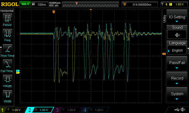 50 Mb/s out signal (blue) sending two different out bytes for each input byte (yellow)
You can see “aA” is sent by the second FPGA board in response to the “a”. There is no idle between these two characters so that’s as fast as you can send two characters in sequence; that’s good. However, on the computer I would only receive an “a” while on the first FPGA board I would see “97” (“a”) and “65” (“A”). So this shows that the first FPGA board is receiving both “a” and “A” but both characters not getting back to the PC. It’s pretty obvious that it’s because the slow transmit UART can’t keep up with the fast rate of the 50 Mb/s UART and has no FIFO. To fix this issue I created the simplest FIFO I could think of…
`ifndef FIFO_UART_TX_H
`define FIFO_UART_TX_H
module fifo_uart_tx
#(
	parameter ApproxDepth = 16,//exact if == 2^N
	parameter Width = 8
)
(
	input clk,

	input [Width-1:0] data_in,
	input data_in_write,

	output reg [Width-1:0] data_out,
	input data_out_read,

	output reg fifo_full,
	output reg fifo_empty
);

localparam Depth=1<<$clog2(ApproxDepth);
localparam bitsNeeded=$clog2(Depth);
reg [bitsNeeded-1:0] buffer_in_ptr=0;
reg [bitsNeeded-1:0] buffer_out_ptr=0;
reg [Width-1:0] buffer [Depth];

wire fifo_full_wire;
wire fifo_empty_wire;
assign fifo_full_wire=(((bitsNeeded)'(buffer_in_ptr+1'b1))==buffer_out_ptr);
assign fifo_empty_wire=(buffer_in_ptr==buffer_out_ptr);

//connect output directly to sync ram
always @(*)
begin
	data_out=buffer[buffer_out_ptr];
	fifo_full=fifo_full_wire;
	fifo_empty=fifo_empty_wire;
end

//update ptrs for rd and wr and write if needed
always @(posedge clk)
begin
	if(data_in_write)
	begin
		if(!fifo_full_wire)
		begin
			buffer[buffer_in_ptr]<=data_in;
			buffer_in_ptr<=buffer_in_ptr+1'b1;
		end
	end
	if(data_out_read)
	begin
		if(!fifo_empty_wire)
		begin
			buffer_out_ptr<=buffer_out_ptr+1'b1;
		end
	end
end

endmodule

`endif
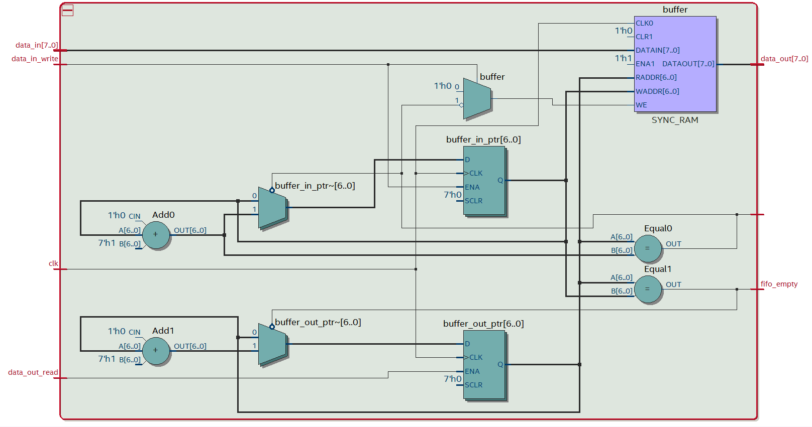 FIFO buffer schematic
This FIFO uses synchronous ram inside the FPGA and a couple of circular pointers to keep track of where to read and write. I gave it minimal RTL simulation validation and it seems to work fine. However I am aware of all FPGAs have synchronous ram so may be this would be more appropriate if you didn’t have it…
always @(posedge clk)
begin
	if(data_in_write)
	begin
		if(!fifo_full_wire)
		begin
			buffer[buffer_in_ptr]<=data_in;
			buffer_in_ptr++;
		end
	end
	data_out<=buffer[buffer_out_ptr];
	if(data_out_read)
	begin
		if(!fifo_empty_wire)
		begin
			buffer_out_ptr++;
		end
	end
	fifo_full<=fifo_full_wire;
	fifo_empty<=fifo_empty_wire;
end
Either way this changes the slow tx UART to the following…
`include "bit_tick.sv"
`include "fifo_uart_tx.sv"

module uart_slow_tx
#(
	parameter ClkFrequency = 50000000, // 50MHz
	parameter Baud = 115200,
	parameter Max_error=0.01, //1%
	parameter FIFO_ApproxDepth=128//exact if == 2^N
)
(
	input clk,
	input [7:0] txbyte,
	input txload,
	output reg txd,//signal out
	output fifo_full
);

reg [7:0] shift_reg=~0;
reg shift_reg_empty=1;
reg [3:0] shift_reg_ptr=8;
initial txd=1;

//bit strobe for enable
wire txstrobe;
bit_tick
#(
	.ClkFrequency(ClkFrequency),
	.Baud(Baud),
	.Max_error(Max_error)
)
uarttx0_bit_tick
(
	.clk_in(clk),
	.tick_out(txstrobe)
);

//fifo for buffering
localparam Width=8;
wire [Width-1:0] data_out;
reg data_out_read;
wire fifo_empty;
fifo_uart_tx
#(
	.ApproxDepth(FIFO_ApproxDepth),
	.Width(Width)
)
fifo0(
.clk(clk),
.data_in(txbyte),
.data_in_write(txload),
.data_out(data_out),
.data_out_read(data_out_read),
.fifo_full(fifo_full),
.fifo_empty(fifo_empty)
);

always @(posedge clk)
begin
	data_out_read<=0;
	if(txstrobe)
	begin

		//send either shift reg or idle
		if(shift_reg_ptr<=7)
		begin
			txd<=shift_reg[shift_reg_ptr];
			shift_reg_ptr<=shift_reg_ptr+1;
		end
		else
		begin
			shift_reg_empty<=1;
			txd<=1;
		end

//this can be 20ns faster but not often. not really worth the effort for the slow uart

		//if load, fifo empty and shift_reg_empty then start sending it
		if(txload&&fifo_empty&&shift_reg_empty)
		begin
			shift_reg<=txbyte;
			shift_reg_ptr<=0;
			txd<=0;
			shift_reg_empty<=0;
			data_out_read<=1;
		end
		//else if the shift reg has gone empty then start sending the next fifo one if available
		else if(shift_reg_empty&&!fifo_empty)
		begin
			shift_reg<=data_out;
			data_out_read<=1;
			shift_reg_ptr<=0;
			txd<=0;
			shift_reg_empty<=0;
		end

// this will work fine and is easier
//
//		//load any data from fifo and advace read pointer
//		if(shift_reg_empty&&!fifo_empty)
//		begin
//			shift_reg<=data_out;
//			data_out_read<=1;
//			shift_reg_ptr<=0;
//			txd<=0;
//			shift_reg_empty<=0;
//		end

	end
end

endmodule
Loading this to the first FPGA board causes the desired response of “aA” when sending an “a”.
Likewise the same FIFO can be added to the fast tx UART…
`include "fifo_uart_tx.sv"

module uart_fast_tx
#(
	parameter FIFO_ApproxDepth=128//exact if == 2^N
)
(
	input clk,//baud rate
	input [7:0] txbyte,
	input txload,
	output reg txd,//signal out
	output fifo_full
);

reg [7:0] shift_reg=~0;
reg shift_reg_empty=1;
reg [3:0] shift_reg_ptr=8;
initial txd=1;

//fifo for buffering
localparam Width=8;
wire [Width-1:0] data_out;
reg data_out_read;
wire fifo_empty;
fifo_uart_tx
#(
	.ApproxDepth(FIFO_ApproxDepth),
	.Width(Width)
)
fifo0(
.clk(clk),
.data_in(txbyte),
.data_in_write(txload),
.data_out(data_out),
.data_out_read(data_out_read),
.fifo_full(fifo_full),
.fifo_empty(fifo_empty)
);

always @(posedge clk)
begin
	data_out_read<=0;

	//send either shift reg or idle
	if(shift_reg_ptr<=7)
	begin
		txd<=shift_reg[shift_reg_ptr];
		shift_reg_ptr<=shift_reg_ptr+1;
	end
	else
	begin
		shift_reg_empty<=1;
		txd<=1;
	end

	//if load, fifo empty and shift_reg_empty then start sending it
	if(txload&&fifo_empty&&shift_reg_empty)
	begin
		shift_reg<=txbyte;
		shift_reg_ptr<=0;
		txd<=0;
		shift_reg_empty<=0;
		data_out_read<=1;
	end
	//else if the shift reg has gone empty then start sending the next fifo one if available
	else if(shift_reg_empty&&!fifo_empty)
	begin
		shift_reg<=data_out;
		data_out_read<=1;
		shift_reg_ptr<=0;
		txd<=0;
		shift_reg_empty<=0;
	end

end

endmodule
I then wanted to see what would happen if the first FPGA was sending a character at the same time as receiving one and whether or not they would interfere with one another. To do this I added the following code to the top level design of the first board to intercept characters between the PC and the second FPGA board…
reg [1:0] bytecount=0;
reg dubbleoutput=0;
always @(posedge clk_slow)
begin
	tx_fpga_byte_valid<=bytecount[0];
	if(|bytecount)
	begin
		bytecount<=bytecount+1;
		if((tx_fpga_byte>=97)&&(tx_fpga_byte<=122))
		begin
			tx_fpga_byte<=tx_fpga_byte-32;//if sending 2 bytes then caps the second byte
		end
	end
	else
	begin
		if(rx_pc_byte_valid)
		begin
			tx_fpga_byte<=rx_pc_byte;
			tx_fpga_byte_valid<=1;
			if(dubbleoutput)bytecount<=2;
			case(rx_pc_byte)
			50: //send 2 bytes for each byte received
			begin
				dubbleoutput<=~dubbleoutput;
			end
			default:
			;
			endcase
		end
	end
end
When enabled by pressing “2” it will send two characters to the second FPGA board for each character receives from the PC. Looking at this on the scope I saw the following…
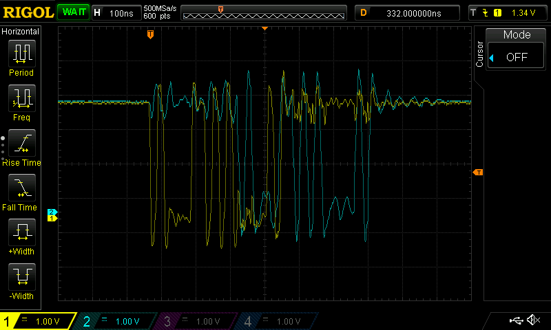 50Mb/s in/out: Two input bytes and two output bytes with signal overlap
You can see that both the first and second FPGA boards are sending data via the fast UARTs at the same time. Holding my finger down on button “a” very occasionally I would get the sequence “aI” or “aE” instead of “aA”. This seemed to be on the order of one in 2000 characters but seemed also much more likely to happen when the oscilloscope was off and attach to the UART wires. This made it very difficult to capture one of these errors on the oscilloscope. I figured out that some characters were more likely to fail than others and “S” seemed to be a good one sometimes producing “[“ instead of “S”. The screenshot below I have finally managed capture one of these errors…
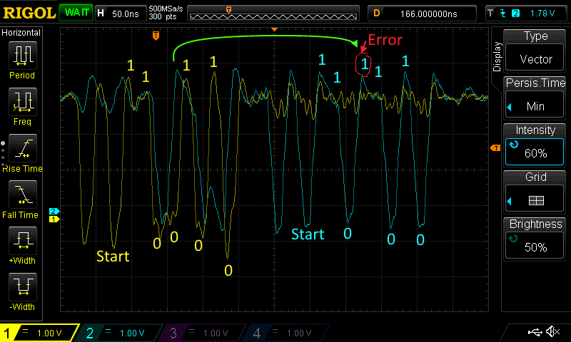 50Mb/s in/out: Two input bytes and two output bytes with signal overlap with reception error!!!
The first FPGA board has sent “S” (start,11001010,stop) but the second FPGA board has sent “[“ (start,11011010,stop). You can see that there is only one bit difference. What’s interesting is when the second FPGA would have sampled the line for this bit as depicted with the green arrow. When the second FPGA was sampling the line for this erroneous bit it was outputting a fast transition from a low to a high of its transmission own UART. So it seems plausible that the reason the second FPGA board outputted the wrong value was because interference from the output of its transmission UART. Interestingly when taking off the oscilloscope probes I would get “{“ instead of “[“. Holding the wires in my hand or connecting the program up to the second board I would get no errors and everything worked flawlessly. Also interestingly increasing the synchronizer of the fast UART by one for the second FPGA board also seemed to fix the problem; maybe the interference causes more probability of metastability? Whatever the case with a synchronizer 2.5 ns longer this 50 Mb/s UART seems to be reliable and I see no strange behavior. So with that as a solution I am calling this 50 Mb/s UART done.
Finally
This is been my first foray into FPGA boards and I found them interesting. This writing documents what I go through when I do something. There are always strange diversions, mistakes, dead ends, and problems along the way; sometimes I solve them sometimes I don’t. Things need not be in order as long as I make progress and learn. So far I’ve only used Altera/Intel ones. I have ordered a Xilinx one but even after two months it still hasn’t arrived. So all I can comment on is what I’ve seen using Altera/Intel. The IDE is pretty weird, clunky, a bit buggy, and quite a steep learning curve. Verilog is also pretty weird, clunky, feels very old-fashioned, and is quite constrictive. The lack of good preprocessing that I’m used to in programming languages is probably my biggest gripe about Verilog, the other thing is having to write begin and end all the time, that’s the reason I don’t use Pascal. It’s really interesting how FPGA feels a cross between electronics in the 80s and insanely complicated electronics of the 20s. It makes me feel a lot like when I was a child sitting on the floor in the corner of a room with a breadboard, some 4000 CMOS logic gates that I had been given, and was connecting wires to them to figure out what they did; that’s really weird. Certainly if you like learning, puzzles, are a control freak or the minutiae of electronics or computers interest you, FPGAs might be for you. For me I’m pleased that I managed to get 50 Mb/s UART working and from what I can see is the fastest UART out there. There might be ones faster that I don’t know about or there may be ones faster in the future yet to come. Either way it’s a crazy thing to have a 50Mb/s UART; at this speed it’s a thousand times faster than dial-up modem. I can think of no reason for doing this except to be able to say you’ve done it much like people who overclock PCs by using liquid nitrogen. It’s all totally crazy but fun. Yes, you might be able to get one going faster but I’ll leave that to you. You can see the problem with UARTs and other asynchronous communication is you have to oversample which is a problem. I oversample eight times, you might be able to use four so you can get up to 100Mb/s but I haven’t tried that and I think four is a little on the low side. Anyway that’s me for now.
Jonti 2020
Home